Array substrate, touch display panel and display device

An array substrate, touch technology, applied in instruments, computing, electrical and digital data processing, etc., to achieve the effect of eliminating reflection

Active Publication Date: 2015-07-15
SHANGHAI TIANMA MICRO ELECTRONICS CO LTD +1
View PDF5 Cites 23 Cited by
  • Summary
  • Abstract
  • Description
  • Claims
  • Application Information

AI Technical Summary

Problems solved by technology

[0004] The technical problem to be solved by the embodiments of the present invention is the visible problem of graphics caused by the backlight reflected by the touch electrode lines in the prior art

Method used


Image

  • Array substrate, touch display panel and display device
  • Array substrate, touch display panel and display device
  • Array substrate, touch display panel and display device

Examples


Embodiment Construction

[0028] In order to make the above-mentioned objects, features and advantages of the present invention more obvious and understandable, the specific embodiments of the present invention will be described in detail below with reference to the accompanying drawings.

[0029] In the following description, many specific details are set forth in order to fully understand the present invention, but the present invention can also be implemented in other ways different from those described herein, so the present invention is not limited by the specific embodiments disclosed below.

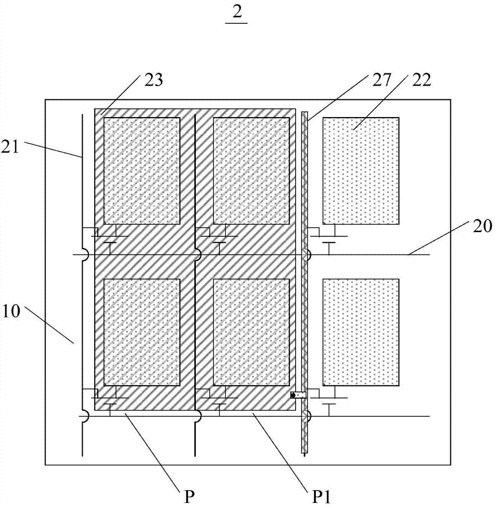
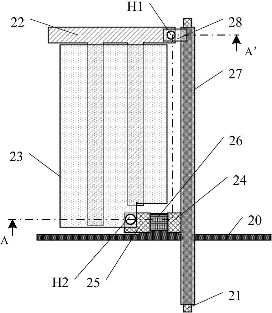
[0030] First describe the structure of P1 and P2 of the array substrate 2 in an embodiment, (Figure 2, 35, middle com structure)

[0031] Then, the structure of the array substrate 3 in another embodiment is basically the same as that of 2, except that P1... (Figure 4, middle com structure)

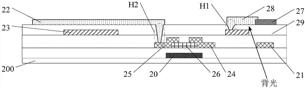
[0032] Last description top com

[0033] Such as figure 1 As shown, the embodiment of the present invention provides an array ...


PUM


Abstract

The invention provides an array substrate. The array substrate comprises a base plate, a plurality of gate lines, a plurality of data lines and a plurality of pixel units defined by the gate lines and the data lines, wherein the pixel units comprise a first pixel unit; the first pixel unit comprises a first insulating layer, at least one common electrode and at least one pixel electrode, at least one first transparent connecting block and at least one touch metal wire; the first insulating layer comprises at least one first through hole; the common electrodes and the pixel electrodes are respectively arranged on two sides of the first insulating layer; the first transparent connecting blocks and the pixel electrode are arranged in the same layer, and each first transparent connecting block is connected with the common electrode through the first through holes; the touch metal wires and the pixel electrode are arranged in the same layer, and each touch metal wire is electrically connected with each first transparent connecting block. The invention also provides a touch display panel and a display device, including the array substrate. According to the array substrate, the touch display panel and the display device provided by the invention, reflection for backlight is eliminated, and the problem of diagram visibility caused by reflection backlight of touch electrode wires is solved.

Description

Technical field [0001] The invention relates to the field of touch display, in particular to an array substrate, a touch display panel and a display device. Background technique [0002] Currently, with the increasing progress of display technology, people not only hope that the display device has the function of displaying images, but also hope that the display device has the function of touch control. Nowadays, touch display devices such as mobile phones, tablet computers, and touch display panels are deeply loved by people. In order to be thinner and lighter, the current touch display device generally integrates touch electrodes on a display panel, such as a color film substrate, an array substrate, an organic light emitting panel, etc. [0003] The pixel structure of the in-cell touch screen in the prior art generally includes a pixel electrode, a common electrode, an insulating layer, and a touch trace. Wherein, the pixel electrode and the common electrode are arranged on bo...

Claims


Application Information

Patent Timeline
Patent Type & Authority Applications(China)
IPC IPC(8): G06F3/041G02F1/1333
CPCG06F3/0412G06F2203/04103G06F3/0443
Inventor 卢峰周星耀丁洪
Owner SHANGHAI TIANMA MICRO ELECTRONICS CO LTD
Why Eureka
Try Eureka