A display substrate and its preparation method, display panel and display device

A display substrate and display panel technology, which is applied in semiconductor/solid-state device manufacturing, semiconductor devices, electrical components, etc., can solve the problems of affecting the holding state and vertical crosstalk of the display screen, so as to improve flatness, avoid capacitive coupling, and eliminate The effect of vertical crosstalk

Active Publication Date: 2018-03-16
BOE TECH GRP CO LTD +1
View PDF4 Cites 0 Cited by
  • Summary
  • Abstract
  • Description
  • Claims
  • Application Information

AI Technical Summary

Problems solved by technology

Although the thin film transistor is not conducting, the capacitive coupling between the data line and the pixel electrode will also affect the holding state of the pixels D1-Dn in the rows G2-Gm, thus causing vertical crosstalk on the display screen
Moreover, the above problems are exacerbated when the resolution is higher

Method used


Image

  • A display substrate and its preparation method, display panel and display device
  • A display substrate and its preparation method, display panel and display device
  • A display substrate and its preparation method, display panel and display device

Examples


Embodiment 1

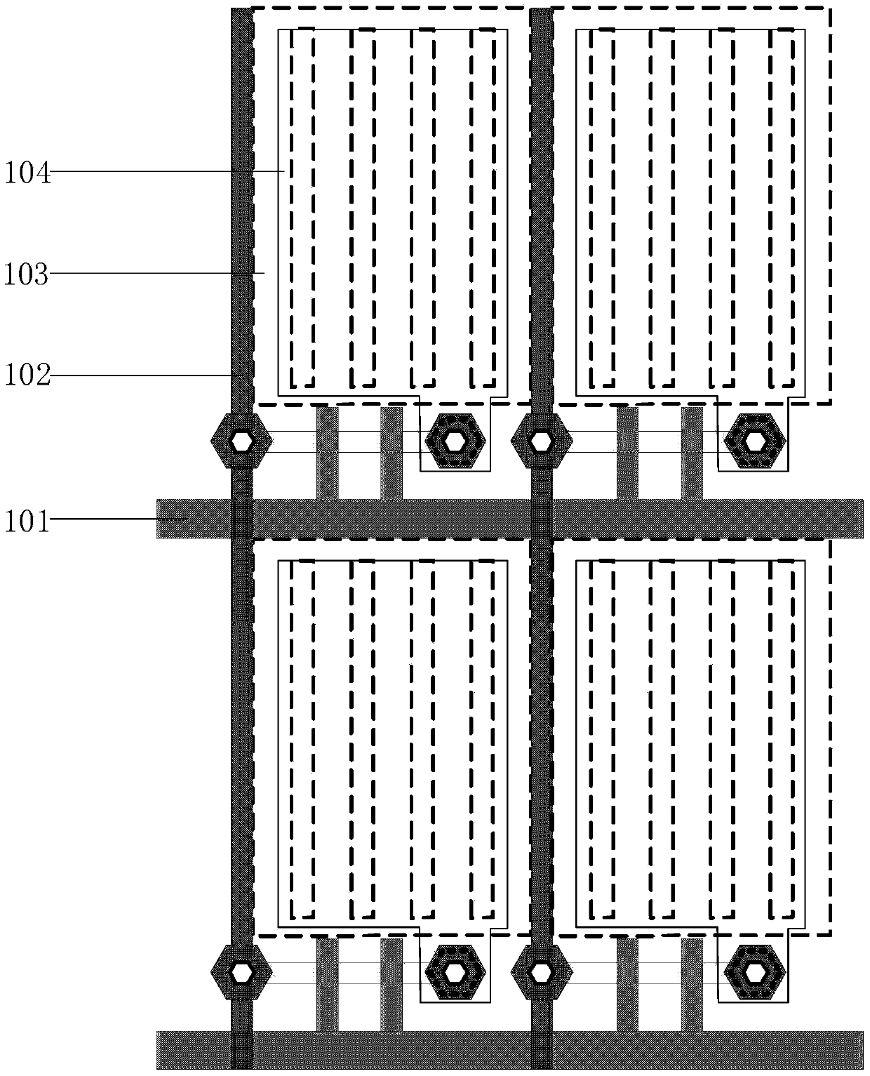
[0035] Figure 4 It is a schematic structural diagram of a display substrate provided in Embodiment 1 of the present invention. It can be understood that the display substrate in this embodiment may be a low-temperature polysilicon display substrate, an oxide display substrate, an a-Si display substrate, or the like. Such as Figure 4 As shown, the display substrate includes a base substrate on which a plurality of first thin film transistors, a plurality of gate lines 101 and a plurality of data lines 102 are arranged. The data line includes at least two data line segments, a second thin film transistor is arranged between adjacent data line segments, a first electrode of the second thin film transistor is connected to a data line segment, and a second thin film transistor of the second thin film transistor is connected to a data line segment. The electrodes are connected to another data line segment, the first electrode is a source and the second electrode is a drain, or t...

Embodiment 2

[0046] This embodiment provides a display panel, including the display substrate provided in the first embodiment above. For details, reference may be made to the description of the first embodiment above, which will not be repeated here.

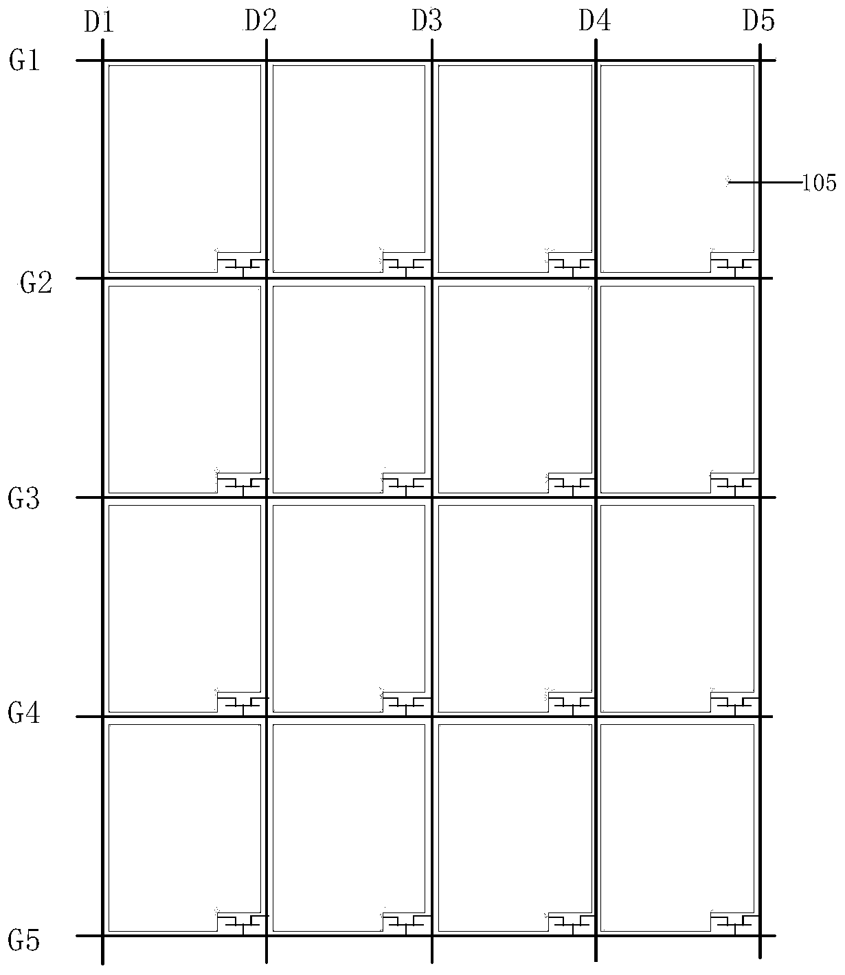
[0047] In the display panel provided in this embodiment, the display substrate includes a base substrate, and a plurality of first thin film transistors, a plurality of gate lines, and a plurality of data lines are arranged on the base substrate, and the data lines include at least two a data line segment, a second thin film transistor is arranged between adjacent data line segments, the first electrode of the second thin film transistor is connected to one data line segment, and the second electrode of the second thin film transistor is connected to another data line segment , so that the data signal is conducted downward under the control of the second thin film transistor, thereby avoiding the capacitive coupling effect between the data l...

Embodiment 3

[0049] This embodiment provides a display device, including the display panel provided in the first embodiment above. For details, reference may be made to the description of the above embodiment, which will not be repeated here.

[0050] In the display device provided in this embodiment, the display substrate includes a base substrate, and the base substrate is provided with a plurality of first thin film transistors, a plurality of gate lines, and a plurality of data lines, and the data lines include at least two a data line segment, a second thin film transistor is arranged between adjacent data line segments, the first electrode of the second thin film transistor is connected to one data line segment, and the second electrode of the second thin film transistor is connected to another data line segment , so that the data signal is conducted downward under the control of the second thin film transistor, thereby avoiding the capacitive coupling effect between the data line and...


PUM


Abstract

The invention discloses a display substrate and a preparation method thereof, a display panel and a display device. The display substrate includes a base substrate, on which a plurality of first thin film transistors, a plurality of gate lines and a plurality of data lines are arranged, and the data lines include at least two data line segments, and adjacent data line segments A second thin film transistor is arranged between them, the first electrode of the second thin film transistor is connected to one data line segment, and the second electrode of the second thin film transistor is connected to another data line segment, so that the data signal is connected to the second The thin film transistor controls the downward conduction of the next level, thereby avoiding the capacitive coupling between the data line and the pixel electrode, completely eliminating the vertical crosstalk, and improving the brightness unevenness at the beginning and end of the scan.

Description

technical field [0001] The present invention relates to the field of display technology, in particular to a display substrate and a preparation method thereof, a display panel and a display device. Background technique [0002] figure 1 It is a schematic diagram showing the structure of the substrate in the prior art. Such as figure 1 As shown, the display substrate includes a base substrate, on which a plurality of gate lines 101 and a plurality of data lines 102 are arranged, and the gate lines 101 and the data lines 102 intersect to define pixel units, so The pixel unit includes a common electrode 103, a pixel electrode 104 and a thin film transistor, the data line 102 is connected to the source of the thin film transistor, and the pixel electrode is connected to the drain of the thin film transistor. [0003] figure 2 It is a structural schematic diagram of a pixel structure in the prior art. Such as figure 2 As shown, the pixel structure includes a pixel unit 10...

Claims


Application Information

Patent Timeline
Patent Type & Authority Patents(China)
IPC IPC(8): H01L27/12H01L21/77
Inventor 辛燕霞杨玉清杨小飞代科
Owner BOE TECH GRP CO LTD
Why Eureka
Try Eureka