Liquid crystal display panel and pixel array substrate thereof

A pixel array substrate and substrate technology, applied in optics, instruments, electrical components, etc., can solve the problems of high resolution and sacrifice of pixel aperture ratio, and achieve the effect of improving aperture ratio

Inactive Publication Date: 2014-01-01
HANNSTAR DISPLAY CORPORATION
View PDF5 Cites 6 Cited by
  • Summary
  • Abstract
  • Description
  • Claims
  • Application Information

AI Technical Summary

Problems solved by technology

However, when portable products using small-size panels (such as 5.3 inches, 5 inches, 4.7 inches, 4.3 inches, etc.) need to be equipped with high resolution, the aperture ratio of the pixels will be forced to a certain degree when the resolution is increased. sacrifice

Method used


Image

  • Liquid crystal display panel and pixel array substrate thereof
  • Liquid crystal display panel and pixel array substrate thereof
  • Liquid crystal display panel and pixel array substrate thereof

Examples


Embodiment Construction

[0083] Below in conjunction with accompanying drawing, structural principle and working principle of the present invention are specifically described:

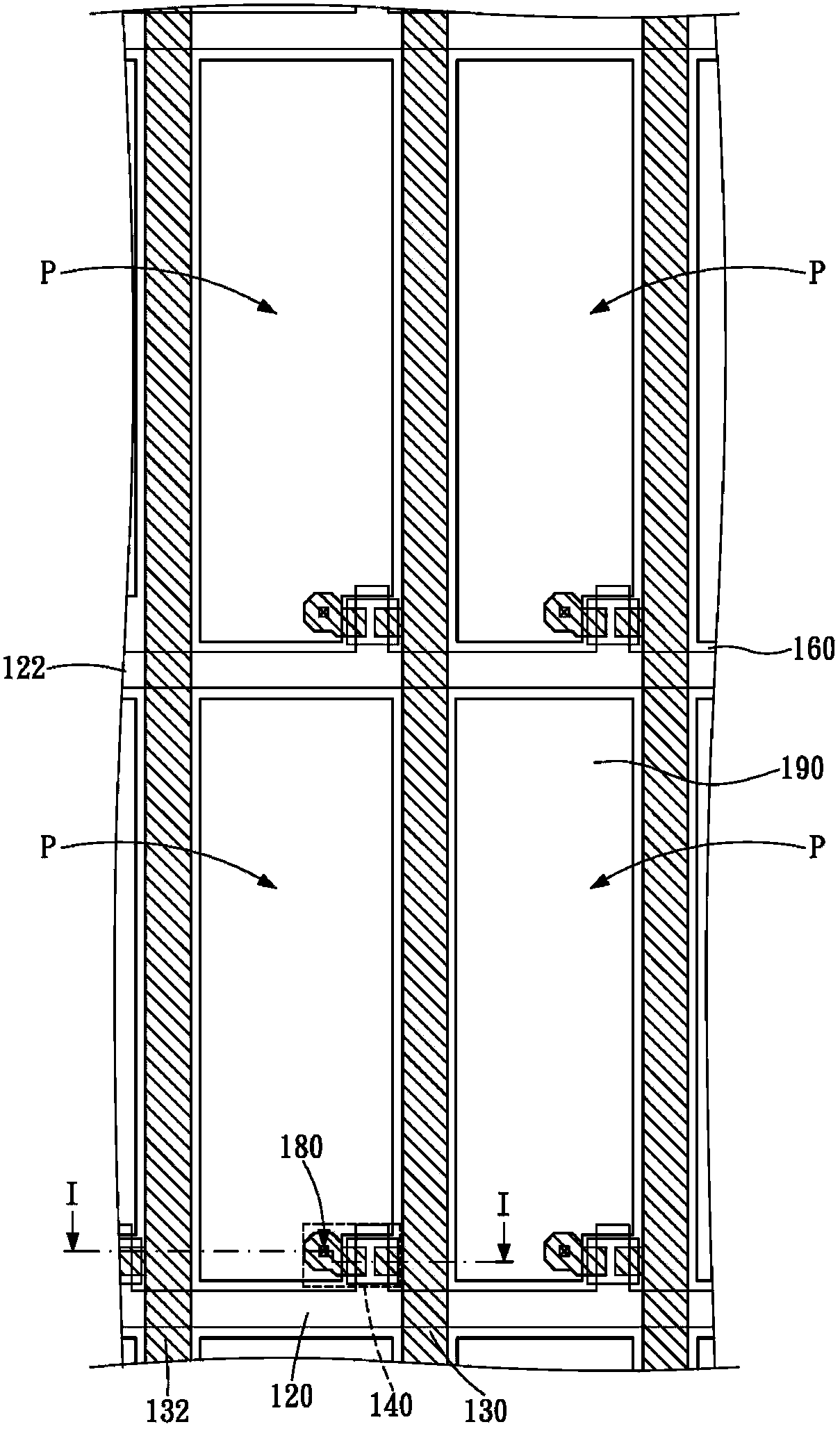
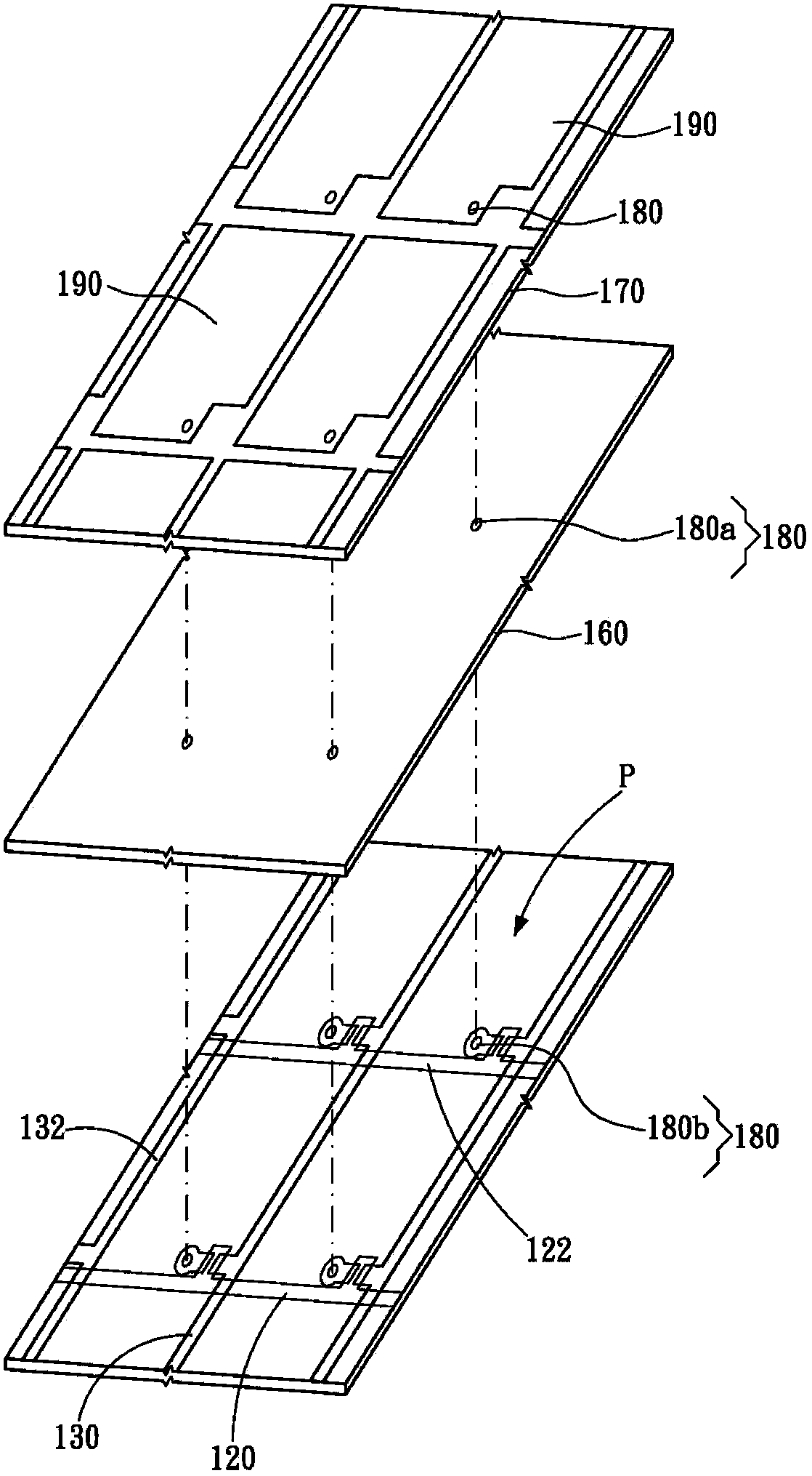
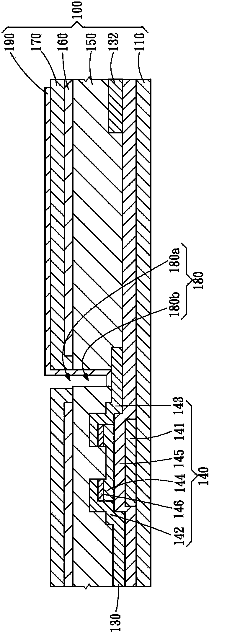
[0084] Figure 1A It is a top view of the pixel array substrate according to the first embodiment of the present invention. Figure 1B for Figure 1A An exploded schematic of the pixel array substrate shown. Figure 1C for Figure 1A The shown cross-sectional view of the pixel array substrate along the line I-I. For the convenience of explanation, Figure 1A The pixel array substrate shown in FIG. 2 omits the drawing of various insulating layers.

[0085] refer to Figure 1A , Figure 1B and Figure 1C , The pixel array substrate 100 includes: a first substrate 110, a plurality of gate lines 120, 122, a plurality of data lines 130, 132, a plurality of thin film transistors 140, a first insulating layer 150, a transparent conductive layer 160, a first Two insulating layers 170 , a plurality of contact holes 180 and a plural...


PUM

PropertyMeasurementUnit
transmittivityaaaaaaaaaa

Abstract

A liquid crystal display panel including on a first substrate (100), gate lines (120,122), data lines (130,132), thin film transistors (140), a first insulation layer (150), a transparent conductive layer (160), a second insulation layer (170), contact holes (180), and pixel electrodes (190). The transparent conductive layer (160) is disposed on the first insulation layers (150) and has a common voltage level. The second insulation layer (170) is disposed between the transparent conductive layer (160) and the pixel electrodes (190). The pixel electrodes (190) are coupled electrically to terminals of the corresponding thin film transistors (140) through the corresponding contact holes (180).

Description

technical field [0001] The invention relates to a liquid crystal display technology, in particular to a liquid crystal display panel and a pixel array substrate thereof. Background technique [0002] In recent years, flat panel displays have developed more and more rapidly, and have gradually replaced traditional cathode ray tube displays. Today's flat-panel displays mainly include the following types: organic light-emitting diode displays (organic light-emitting diodes display; OLED), plasma displays (plasma display panel; PDP), liquid crystal displays (liquid crystal display; LCD), and field emission displays (field emission display; FED) and so on. Among them, the liquid crystal display technology can be divided into two types according to the twisting mode of the liquid crystal molecular material. One is twisted nematic LCD (TN-LCD), and the other is in-plane switching liquid crystal display (IPS-LCD). In TN-LCD, the liquid crystal molecules of the liquid crystal disp...

Claims


Application Information

Patent Timeline
Patent Type & Authority Applications(China)
IPC IPC(8): G02F1/1362G02F1/1368H01L27/02
CPCG02F1/136213G02F2001/136218G02F1/136218
Inventor 游家华林松君刘轩辰
Owner HANNSTAR DISPLAY CORPORATION
Why Eureka
Try Eureka