Pixel defining layer structure and fabrication method of oled device

A pixel definition layer and device technology, which is applied in semiconductor/solid-state device manufacturing, semiconductor devices, electric solid-state devices, etc., can solve the problems of unfavorable OLED devices, poor uniformity of device pixels, and reduce device aperture ratio, so as to avoid device open circuit , improve the uniformity and reduce the production cost

Active Publication Date: 2018-11-06
GUANGDONG JUHUA PRINTING DISPLAY TECH CO LTD
View PDF5 Cites 0 Cited by
  • Summary
  • Abstract
  • Description
  • Claims
  • Application Information

AI Technical Summary

Problems solved by technology

[0005] The purpose of the present invention is to provide a method for preparing a pixel defining layer structure, aiming at solving the problem that the existing method for preparing the pixel defining layer structure leads to poor uniformity of device pixels, or even leads to open circuit of the device, reduces the aperture ratio of the device, or is not conducive to the solution method Problems in making OLED devices

Method used


Image

  • Pixel defining layer structure and fabrication method of oled device
  • Pixel defining layer structure and fabrication method of oled device
  • Pixel defining layer structure and fabrication method of oled device

Examples


Embodiment Construction

[0023] In order to make the technical problems, technical solutions and beneficial effects to be solved by the present invention clearer, the present invention will be further described in detail below in conjunction with the accompanying drawings and embodiments. It should be understood that the specific embodiments described here are only used to explain the present invention, not to limit the present invention.

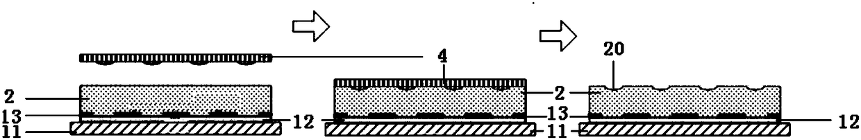
[0024] to combine Figure 3-4 , an embodiment of the present invention provides a method for preparing a pixel defining layer structure, comprising the following steps:

[0025] S01. A TFT backplane 1 is provided, and a negative photoresist layer 2 is coated on the anode 13 of the TFT backplane 1;

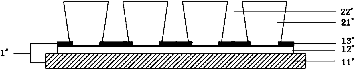
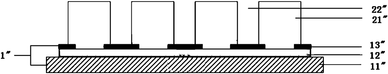
[0026] Specifically, in the above step S01 , the TFT backplane 1 includes a TFT array 12 and an anode 13 sequentially stacked on a hard carrier substrate 11 . The TFT backplane 1 can be one of a rigid TFT backplane or a flexible TFT backplane. When a rigid TFT backpl...


PUM


Abstract

The invention is applicable to the technical field of printing and display, and provides a pixel defining layer structure and a preparation method of an OLED device respectively. The preparation method of the pixel defining layer structure includes the following steps: providing a TFT backplane, coating a negative photoresist layer on the anode of the TFT backplane; Baking, embossing, and post-baking treatment to obtain a negative photoresist layer with a concave embossing pattern on the surface; the mask plate is fixed on the negative photoresist layer, and the light transmission of the mask plate is made The channel is placed directly above the concave embossing pattern, so that the light passing through the light-transmitting channel enters the negative photoresist layer through the concave embossing pattern, and sequentially undergoes exposure, development and etching to obtain The trapezoidal pixel in the inverted trapezoidal pixel region defines a layer structure, wherein the size of the light-transmitting channel of the mask plate is not larger than the size of the concave embossing pattern.

Description

technical field [0001] The invention belongs to the technical field of printing and display, and in particular relates to a pixel defining layer structure and a preparation method of an OLED device. Background technique [0002] OLED display devices are considered to be the next-generation flat-panel display emerging application technology due to their advantages of self-illumination, no need for backlight, high contrast, thin thickness, wide viewing angle, fast response speed, and flexible panels. At present, for the preparation of OLED display devices, vacuum evaporation and printing technologies are usually used to prepare, which is the current international mainstream development technology. The vacuum evaporation technology of small molecules is relatively mature and has been industrialized at present, and small and medium-sized full-color display screens have been launched in batches, which are applied in the fields of electronic equipment such as MP3, MP4, mobile phon...

Claims


Application Information

Patent Timeline
Patent Type & Authority Patents(China)
IPC IPC(8): H01L21/027H01L27/32H01L51/56
CPCH01L21/0274H10K71/00
Inventor 高卓
Owner GUANGDONG JUHUA PRINTING DISPLAY TECH CO LTD
Why Eureka
Try Eureka