Preparation for r-Li ALO2 single-crystal thin-film covering layer substrate by pulsing laser deposition

A technology of pulsed laser deposition and single crystal thin film, which is applied in the direction of single crystal growth, single crystal growth, chemical instruments and methods, etc., can solve the problems of waste of raw materials, difficulty in obtaining large size, difficulty in crystal growth, etc., and achieve the effect of reducing costs

Inactive Publication Date: 2005-05-11
SHANGHAI INST OF OPTICS & FINE MECHANICS CHINESE ACAD OF SCI
View PDF1 Cites 0 Cited by
  • Summary
  • Abstract
  • Description
  • Claims
  • Application Information

AI Technical Summary

Problems solved by technology

[0006] The aforementioned prior art substrate (α-Al 2 o 3 , Si or γ-LiAlO 2 ) The significant disadvantages that exist are: (1) use α-Al 2 o 3 , silicon, etc. as the substrate, the lattice mismatch between the substrate and GaN is high, so that the prepared GaN film has a high dislocation density and a large number of point defects; (2) due to LiAlO 2 Non-stoichiometric volatilization is prone to occur at high temperature in the melt, crystal growth is difficult, and it is difficult to obtain large-size, high-quality LiAlO 2 Single crystal, the largest sapphire diameter reaches 350mm, while LiAlO 2 The diameter of the substrate is less than 100mm, and the processing of the substrate will cause a lot of waste of raw materials

Method used


Image

  • Preparation for r-Li ALO2 single-crystal thin-film covering layer substrate by pulsing laser deposition

Examples


Embodiment 1

[0025] Weigh a certain amount of LiOH and Al 2 o 3 (molar ratio 2:1) put it into a reaction vessel, heat it in an air atmosphere and keep the temperature at 600°C, and fully react for 1.5h (above) to obtain γ-LiAlO 2 . Then γ-LiAlO 2 The powder is pressed into a target;

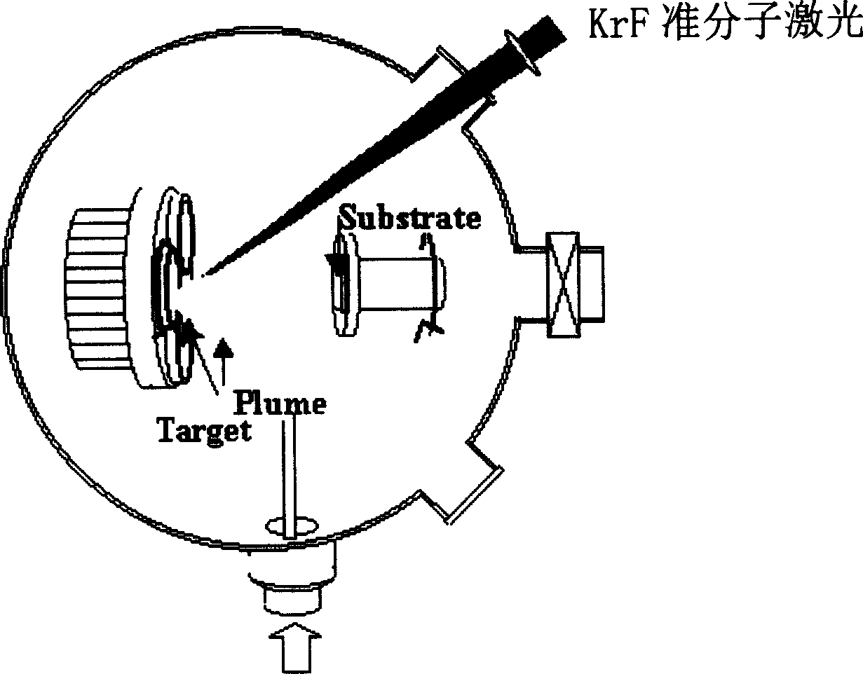
[0026] α-Al to be cleaned 2 o 3 Or silicon substrate and γ-LiAlO 2 The target material is sent into the pulsed laser deposition device;

[0027] Evacuate the cavity into a high vacuum (> 10 -4 Pa), then filled with argon atmosphere;

[0028] Heat the substrate to 500°C, and pass the KrF excimer laser with a pulse width of 25ns through the lens at 10J / cm 2 Concentrate light with an energy density of 1000000000000000000000000000000000000000000000000000000000000000000000000000000000000000000000000000000000000000000000000000000000000000000000000000000000000000000000000000000000000000000000000000000000000000000000000, through the optical window to γ-LiAlO in the device 2 The target material, the surfa...

Embodiment 2

[0030] Weigh a certain amount of LiOH and Al 2 o 3 (molar ratio 2:1) put it into a reaction vessel, heat it in an air atmosphere and keep the temperature at 500°C for a full reaction of 1.5h (above) to obtain γ-LiAlO 2 . Then γ-LiAlO 2 The powder is pressed into a target;

[0031] α-Al to be cleaned 2 o 3 Or silicon substrate and γ-LiAlO 2 The target material is sent into the pulsed laser deposition device;

[0032] Evacuate the cavity into a high vacuum (> 10 -4 Pa), then filled with argon atmosphere;

[0033] Heat the substrate to 600°C, and pass the KrF excimer laser with a pulse width of 25ns through the lens at 10J / cm 2 Concentrate light with an energy density of 1000000000000000000000000000000000000000000000000000000000000000000000000000000000000000000000000000000000000000000000000000000000000000000000000000000000000000000000000000000000000000000000000000000000000000000000000, through the optical window to γ-LiAlO in the device 2 The target material, the surfa...

Embodiment 3

[0035] Weigh a certain amount of LiOH and Al 2 o 3 (molar ratio 2:1) put it into a reaction vessel, heat it in the air atmosphere and keep the temperature at 600°C for a full reaction of 1.5h (above) to obtain γ-LiAlO 2 . Then γ-LiAlO 2 The powder is pressed into a target;

[0036] α-Al to be cleaned 2 o 3 Or silicon substrate and γ-LiAlO 2 The target material is sent into the pulsed laser deposition device;

[0037] Evacuate the cavity into a high vacuum (> 10 -4 Pa), then filled with argon atmosphere;

[0038] Heating the substrate to 900°C, focusing the KrF excimer laser with a certain energy density through the lens, and irradiating the γ-LiAlO in the device through the optical window 2 The target material, the surface layer molecules of the target material are melted and vaporized to form a film on the substrate, and the γ-LiAlO can be obtained after slow cooling 2 single crystal film.

[0039] Experiments show that the method of the invention has simple pr...


PUM


Abstract

This invention relates to preparation of gama-LiAlO2 monocrystal film on alpha-Al2O3 or Si substrate by deposition. It is carried out by: preparing gama-LiAlO2, using laser pulses to vapor surface molecules out of target material, heating the target material, and depositing gama-liAlO2 on it. It is simple and suitable for quality GaN growth on substrate by epitaxial process.

Description

technical field [0001] The present invention is related to the epitaxial growth of InN-GaN-based blue light semiconductor, especially a kind of pulsed laser deposition to prepare γ-LiAlO 2 Single crystal thin film capping layer substrate method. This substrate material is mainly used for epitaxial growth of InN-GaN-based blue light semiconductor. Background technique [0002] Wide bandgap III-V compound semiconductor materials represented by GaN are attracting more and more attention, they have excellent characteristics, such as stable physical and chemical properties, high thermal conductivity and high electron saturation velocity, direct bandgap materials The probability of optical transition is an order of magnitude higher than that of indirect bandgap, so wide bandgap InN-GaN-based semiconductors are widely used in blue and green light-emitting diodes (LEDs) and laser diodes (LDs), high-density information reading and writing, underwater communication, deep water detect...

Claims


Application Information

Patent Timeline
Patent Type & Authority Applications(China)
IPC IPC(8): C30B23/02C30B23/06C30B29/22H01L33/00
Inventor 王银珍徐军周圣明杨卫桥李抒智彭观良刘世良
Owner SHANGHAI INST OF OPTICS & FINE MECHANICS CHINESE ACAD OF SCI
Why Eureka
Try Eureka