Preparation method of display substrate, display substrate and display device

A technology for display substrates and array substrates, applied in semiconductor/solid-state device manufacturing, diodes, semiconductor devices, etc., can solve problems such as the decrease in aperture ratio, achieve the effects of eliminating the decrease in aperture ratio, increasing the aperture ratio, and avoiding preparation

Active Publication Date: 2016-03-30
BOE TECH GRP CO LTD
View PDF5 Cites 38 Cited by
  • Summary
  • Abstract
  • Description
  • Claims
  • Application Information

AI Technical Summary

Problems solved by technology

[0004] The object of the present invention is to provide a method for preparing a display substrate, a display substrate, and a display device, so as to solve the problem of lower aperture ratio caused by fabricating color filters on an array substrate

Method used


Image

  • Preparation method of display substrate, display substrate and display device
  • Preparation method of display substrate, display substrate and display device
  • Preparation method of display substrate, display substrate and display device

Examples


Embodiment 1

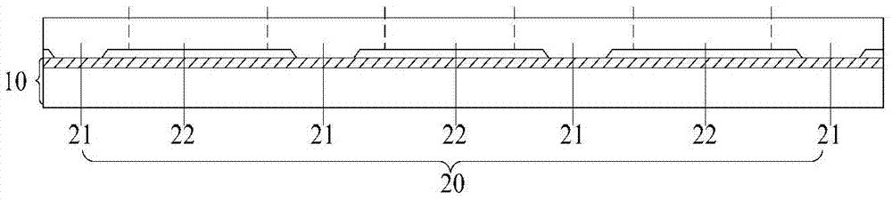
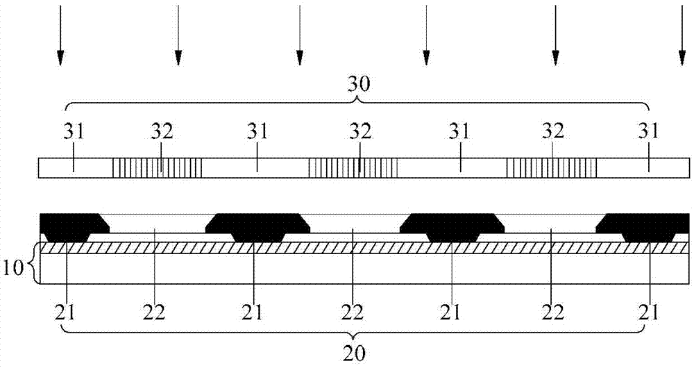
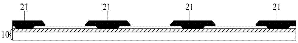
[0026] As mentioned in the background art, in the prior art, the color filter is directly prepared on the array substrate, which complicates the film layer structure of the display substrate, and further reduces the aperture ratio to a certain extent. In order to solve this problem, the inventor thought that: since the pixel defining layer on the array substrate is located in its non-pixel area, and when the color filter is prepared on the array substrate, the black matrix of the color filter is also located on the array substrate. In the non-pixel area, therefore, a pixel-defining layer with light-shielding properties can be prepared to replace the black matrix to play a light-shielding function, so that the black matrix can be removed from the substrate. Starting from this idea of ​​the invention, the inventors of the present invention consider that the pixel defining layer is generally formed by patterning process, and the forming material of the pixel defining layer mainly ...

Embodiment 2

[0061] An embodiment of the present invention provides a display substrate, see Figure 7 and Figure 8 , the display substrate includes an array substrate 10 and a pixel defining layer 40 uniformly distributed with a photochromic material, the pixel defining layer 40 is arranged on the non-pixel area of ​​the array substrate 10, and the photochromic material can be transmitted by light under the action of light The light becomes light-shielding, so that the pixel defining layer containing the photochromic material can change from light-transmitting to light-shielding under the action of light, and the transformation of the pixel defining layer from light-transmitting to light-shielding is irreversible.

[0062] Since the photochromic material is evenly distributed in the pixel defining layer 40 of the above display substrate, the photochromic material can change from light transmission to light shielding under the action of light, so when preparing the pixel defining layer of...

Embodiment 3

[0068] An embodiment of the present invention provides a display device, which includes the display substrate in the second embodiment above.

[0069] In the display substrate of the above-mentioned display device, the photochromic material is evenly distributed in the pixel defining layer, and the photochromic material can change from light transmission to light shielding under the action of light, so that only by exposure, light, etc., the formation of The pixel defining layer has the effect of shading. Therefore, the above-mentioned display device can prepare a light-shielding pixel defining layer through a simple patterning process, and replace the black matrix with the light-shielding pixel defining layer, which simplifies the film layer structure of the display substrate, thereby solving the problem of color filter preparation. On the array substrate, the problem of decreasing the aperture ratio is caused, and the aperture ratio of the display device is improved. At the...


PUM


Abstract

The invention provides a preparation method of a display substrate, the display substrate and a display device, relates to the technical field of display, and aims at solving the problem that the aperture opening ratio is reduced due to the fact that a color light filter is fabricated on an array substrate. The preparation method of the display substrate comprises the steps as follows: a thin-film transistor array is prepared on a substrate to form the array substrate; a pixel definition layer is formed in a non-pixel region of the array substrate by a composition process; photochromic materials are evenly distributed in the pixel definition layer; the pixel definition layer containing the photochromic materials is converted into a shading state from a transmitting state under the action of illumination; and the pixel definition layer is converted into a shading irreversible state from the transmitting state. The preparation method of the display substrate provided by the invention is used for preparing the color light filter on the array substrate.

Description

technical field [0001] The invention relates to the field of display technology, in particular to a method for preparing a display substrate, a display substrate, and a display device. Background technique [0002] Display devices such as Liquid Crystal Display (LCD for short) and Organic Light-Emitting Diode (OLED for short) have become necessities in people's lives. A display device usually includes an array substrate and a color filter (ColorFilter, CF for short) in a box. To solve the problems of decreased aperture ratio and light leakage, a display substrate with both an array substrate and a color filter structure emerges as the times require. The structure of this display substrate includes an array substrate and a color filter formed above the array substrate. Since the process of aligning the array substrate and the color filter to the box is avoided, there is no opening caused by alignment deviation. rate drop and light leakage issues. [0003] However, directly...

Claims


Application Information

Patent Timeline
Patent Type & Authority Applications(China)
IPC IPC(8): H01L21/77H01L27/12H01L27/32H01L51/52H01L51/56
CPCH01L21/77H01L27/12H10K59/00H10K59/122H10K50/80H10K71/00H10K59/38H10K59/126H10K50/865H10K59/50H10K59/1213H10K59/1201
Inventor 李伟宋泳锡方金钢孙宏达
Owner BOE TECH GRP CO LTD
Why Eureka
Try Eureka