Display equipment
A technology for display equipment and display modules, which can be applied to instruments, identification devices, etc., and can solve the problems of poor appearance and light leakage of display equipment.
- Summary
- Abstract
- Description
- Claims
- Application Information
AI Technical Summary
Problems solved by technology
Method used
Image

Examples
Embodiment 1
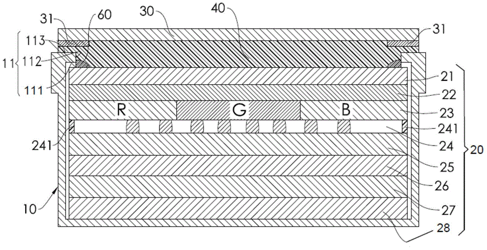
[0031] Such as figure 1 As shown, the display device of this embodiment includes a frame body 10 , a display module 20 , a protective cover 30 , a first adhesive layer 40 and a light blocking component 60 .
[0032] Such as figure 1 and 2 As shown, an upper opening 11 is formed on the upper side of the frame body 10, an opening is formed around the upper opening portion 11, and an accommodating space is formed inside the frame body 10, and the upper opening portion 11 includes an inner surface 111 and an end surface 112 and an outer surface 113 , the end surface 112 is connected and formed between the inner surface 111 and the outer surface 113 .
[0033] The display module 20 is accommodated in the accommodating space of the frame body 10 , and there is a gap between the display module 20 and the upper opening 11 of the frame body 10 . Further, the edge of the upper side of the display module 20 is covered by the upper opening 11 of the frame body 10, the upper side of t...
Embodiment 2
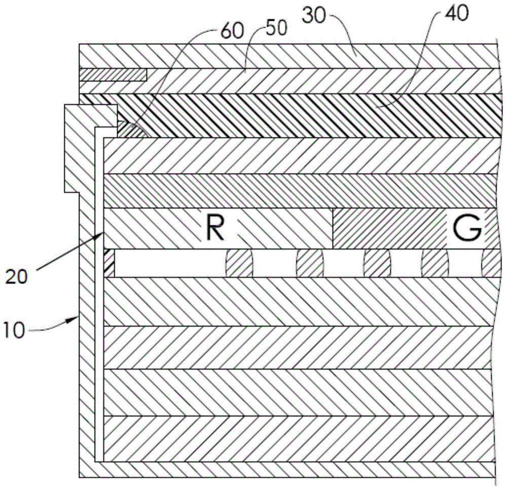
[0039] Such as figure 2 As shown, this embodiment is substantially the same as Embodiment 1. However, the difference between this embodiment and Embodiment 1 is that the display device of this embodiment not only includes the frame body 10, the display module 20, the protective cover 30, the first adhesive layer 40 and the light blocking component 60, but also An inductive conductive structure 50 is included. The inductive conductive structure 50 is disposed between the protective cover 30 and the first adhesive layer 40 to enable the display device of this embodiment to have a touch function. The light-shielding layer 31 simultaneously shields the peripheral wires (not shown) of the sensing conductive structure 50 . It should be noted that in this embodiment, the inductive conductive structure 50 includes a layer of inductive conductive layer, which is directly formed on the surface of the protective cover 30 facing the upper opening 11, but in other embodiments, the induc...
Embodiment 3
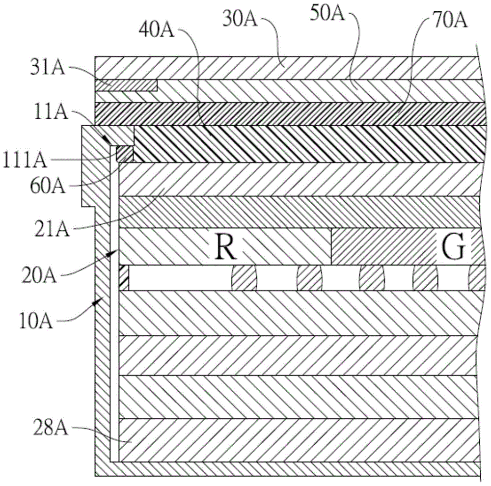
[0041] Such as image 3 As shown, this embodiment is substantially the same as Embodiment 2. However, the difference between this embodiment and Embodiment 1 is that the display device of this embodiment includes a frame body 10A, a display module 20A, a protective cover 30A, a first adhesive layer 40A, a sensing conductive layer 50A and a light-shielding Besides the component 60A, it further includes a second adhesive layer 70A. The second adhesive layer 70A is disposed between the first adhesive layer 40A and the sensing conductive layer 50A, so that the protective cover 30 can be fixed to the frame body 10 at the same time, so as to improve the bonding reliability of the display device. The second adhesive layer 70A is made of liquid transparent optical glue or solid transparent optical glue. There is a certain height difference between the upper side of the frame body 10A and the upper side of the display module 20A. In this embodiment, the height difference is eliminate...
PUM
 Abstract
Description
Claims
Application Information
 - R&D Engineer
- R&D Manager
- IP Professional
- Industry Leading Data Capabilities
- Powerful AI technology
- Patent DNA Extraction
Browse by: Latest US Patents, China's latest patents, Technical Efficacy Thesaurus, Application Domain, Technology Topic.
© 2024 PatSnap. All rights reserved.Legal|Privacy policy|Modern Slavery Act Transparency Statement|Sitemap