Method of making a contact structure with a distinctly formed tip structure
What is AI technical title?
AI technical title is built by Patsnap AI team. It summarizes the technical point description of the patent document.
a tip structure and contact technology, applied in the direction of printed circuit assembling, non-electric welding apparatus, printed element electric connection formation, etc., can solve the problems of dies being “good” (full functional), dies being “bad” (non functional), and certain difficulties inherent in any technique for probing semiconductor dies. , to achieve the effect of convenient control of impedance, convenient demountability and effective shielding
Inactive Publication Date: 2006-08-08
FORMFACTOR INC
View PDF185 Cites 51 Cited by
Summary
Abstract
Description
Claims
Application Information
AI Technical Summary
This helps you quickly interpret patents by identifying the three key elements:
Problems solved by technology
Method used
Benefits of technology
Benefits of technology
[0045]An additional advantage of the present invention is that connections made with the interconnection elements of the present invention are readily demountable. Soldering, to effect the interconnection to a terminal of an electronic component is optional, but is generally not preferred at a system level.
[0046]According to an aspect of the invention, techniques are described for making interconnection elements having controlled impedance. These techniques generally involve coating (e.g., electrophoretically) a conductive core or an entire composite interconnection element with a dielectric material (insulating layer), and overcoating the dielectric material with an outer layer of a conductive material. By grounding the outer conductive material layer, the resulting interconnection element can effectively be shielded, and its impedance can readily be controlled. (See also FIG. 10K of the PARENT CASE.)
[0047]According to an aspect of the invention, interconnection elements can be pre-fabricated as individual units, for later attachment to electronic components. Various techniques for accomplishing this objective are set forth herein. Although not specifically covered in this document, it is deemed to be relatively straightforward to fabricate a machine that will handle the mounting of a plurality of individual interconnection elements to a substrate or, alternatively, suspending a plurality of individual interconnection elements in an elastomer, or on a support substrate.
[0048]It should clearly be understood that the composite interconnection element of the present invention differs dramatically from interconnection elements of the prior art which have been coated to enhance their electrical conductivity characteristics or to enhance their resistance to corrosion.
[0049]The overcoating of the present invention is specifically intended to substantially enhance anchoring of the interconnection element to a terminal of an electronic component and / or to impart desired resilient characteristics to the resulting composite interconnection element. Stresses (contact forces) are directed to portions of the interconnection elements which are specifically intended to absorb the stresses.
[0050]It should also be appreciated that the present invention provides essentially a new technique for making spring structures. Generally, the operative structure of the resulting spring is a product of plating, rather than of bending and shaping. This opens the door to using a wide variety of materials to establish the spring shape, and a variety of “friendly” processes for attaching the “falsework” of the core to electronic components. The overcoating functions as a “superstructure” over the “falsework” of the core, both of which terms have their origins in the field of civil engineering.
Problems solved by technology
In practice, however, certain physical defects in the wafer itself and certain defects in the processing of the wafer inevitably lead to some of the dies being “good” (fully-functional) and some of the dies being “bad” (non-functional).
Certain difficulties are inherent in any technique for probing semiconductor dies.
This ring-shape layout makes it difficult, and in some cases impossible, to probe a plurality of unsingulated semiconductor dies (multiple sites) on a wafer, especially when the bond pads of each semiconductor die are arranged in other than two linear arrays along two opposite edges of the semiconductor die.
As a general proposition, the higher the yield strength of a material, the more difficult it will be to work with (e.g., punch, bend, etc.).
Such “hostile” processes are generally not desirable (and often not feasible) in the context of certain relatively “fragile” electronic components such as semiconductor devices.
However, both solder and gold are relatively soft (low yield strength) materials which will not function well as spring elements.
A subtle problem associated with interconnection elements, including spring contacts, is that, often, the terminals of an electronic component are not perfectly coplanar.
Method used
Image
Click on the blue label to locate the original text in one second.
Reading with bidirectional positioning of images and text.
Examples
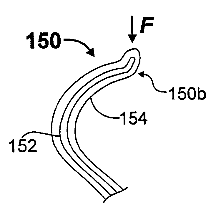
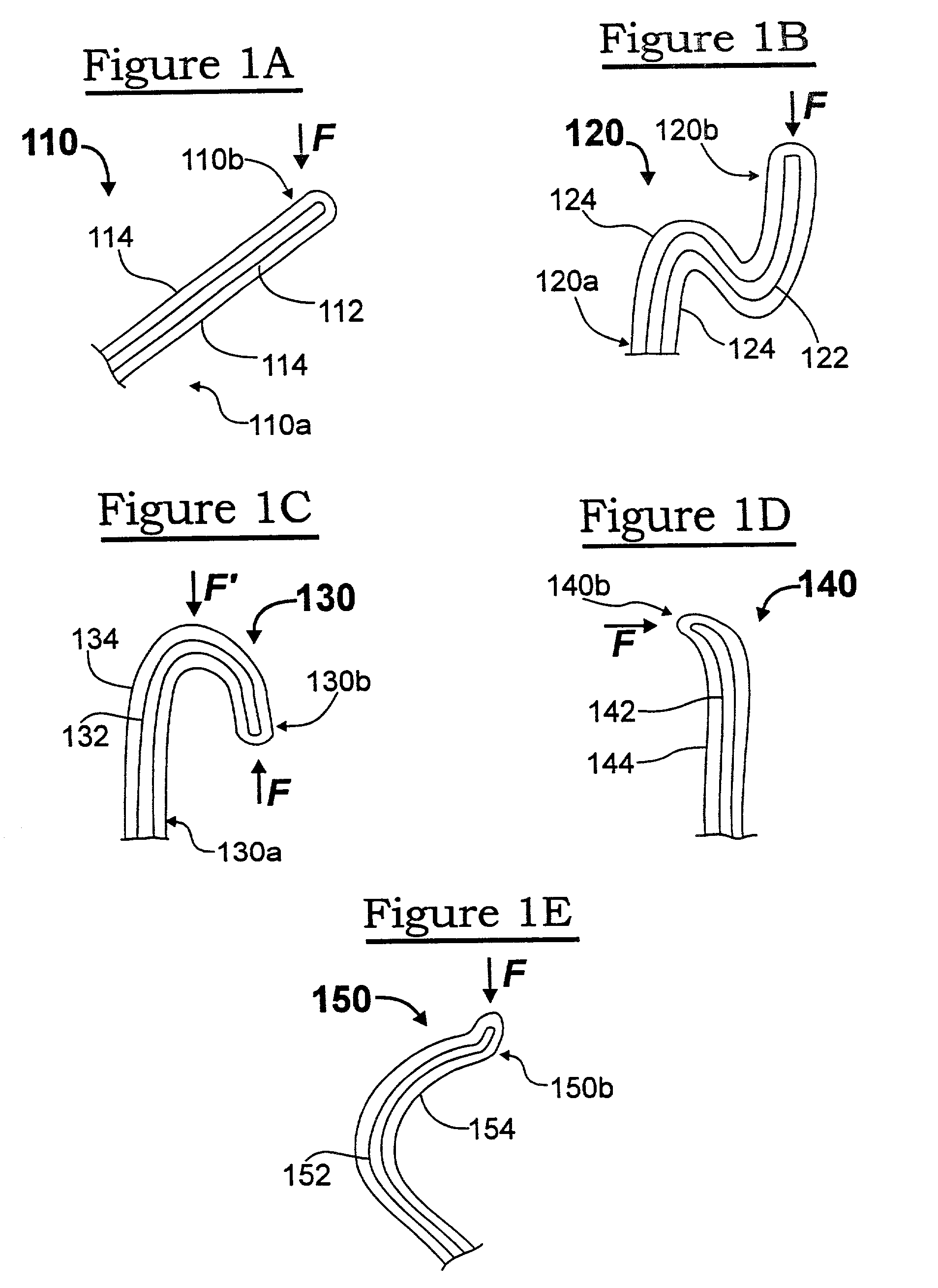
embodiment 200
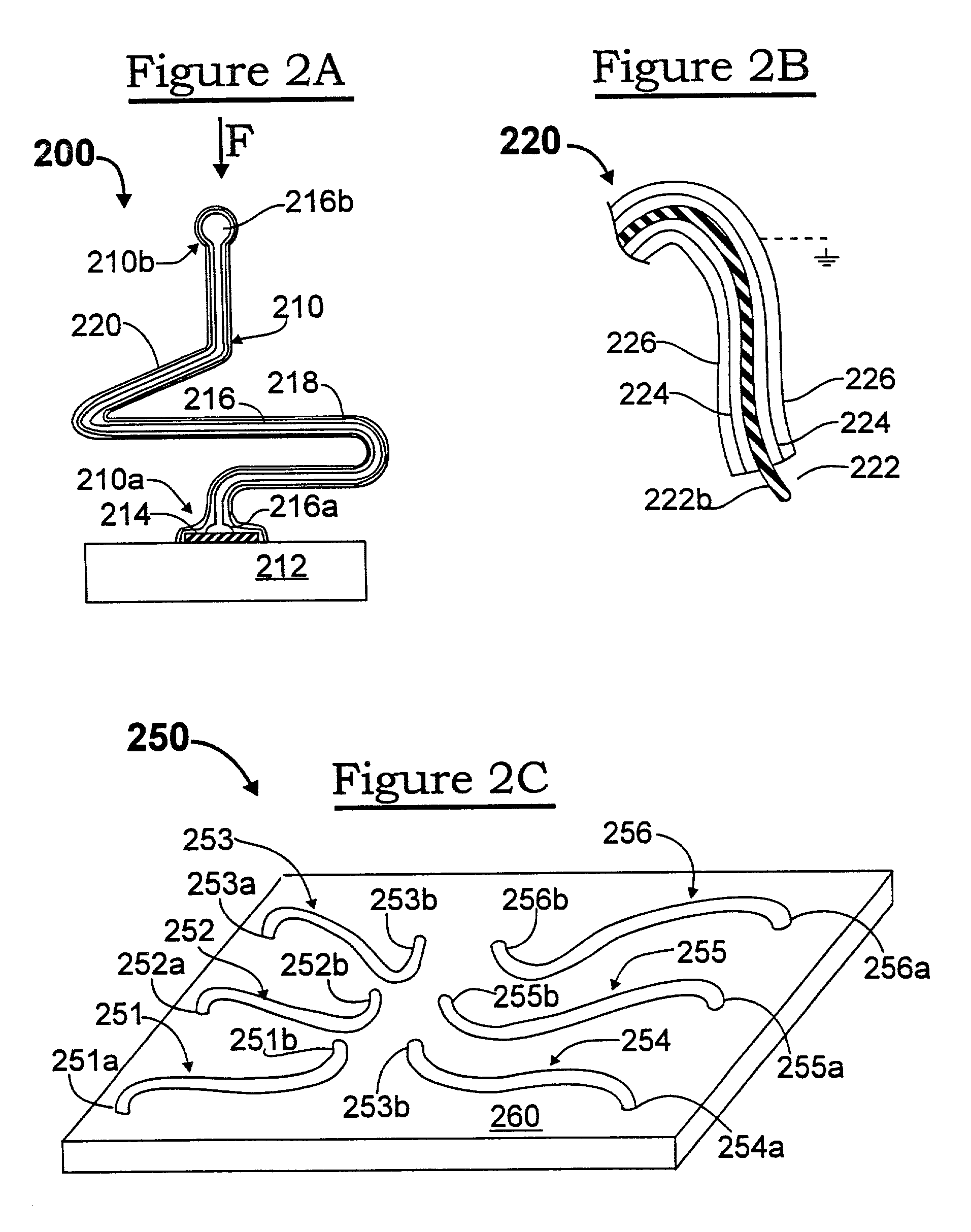
[0113]FIG. 2A illustrates an embodiment 200 of an interconnection element 210 mounted to an electronic component 212 which is provided with a terminal 214. In this example, a soft (e.g., gold) wire core 216 is bonded (attached) at one end 216a to the terminal 214, is configured to extend from the terminal and have a spring shape (compare the shape shown in FIG. 1B), and is severed to have a free end 216b. Bonding, shaping and severing a wire in this manner is accomplished using wirebonding equipment. The bond at the end 216a of the core covers only a relatively small portion of the exposed surface of the terminal 214.
[0114]A shell (overcoat) is disposed over the wire core 216 which, in this example, is shown as being multi-layered, having an inner layer 218 and an outer layer 220, both of which layers may suitably be applied by plating processes. One or more layers of the multi-layer shell is (are) formed of a hard material (such as nickel and its alloys) to impart a desired resilie...
embodiment 250
[0130]FIG. 2C illustrates an embodiment 250 wherein a plurality (six of many shown) of interconnection elements 251 . . . 256 are mounted on a surface of an electronic component 260, such as a probe card insert (a subassembly mounted in a conventional manner to a probe card). Terminals and conductive traces of the probe card insert are omitted from this view, for illustrative clarity. The attached ends 251a . . . 256a of the interconnection elements 251 . . . 256 originate at a first pitch (spacing), such as 0.05–0.10 inches. The interconnection elements 251 . . . 256 are shaped and / or oriented so that their free ends (tips) are at a second, finer pitch, such as 0.005–0.010 inches. An interconnect assembly which makes interconnections from a one pitch to another pitch is typically referred to as a “space transformer”.
[0131]As illustrated, the tips 251b . . . 256b of the interconnection elements are arranged in two parallel rows, such as for making contact to (for testing and / or burn...
embodiment 270
[0146]FIG. 2I illustrates an alternate embodiment 270 for fabricating interconnection elements. In this embodiment, a masking material 272 is applied to the surface of a sacrificial substrate 274, and is patterned to have a plurality (one of many shown) of openings 276, in a manner similar to the technique described hereinabove with respect to FIG. 2D. The openings 276 define areas whereat interconnection elements will be fabricated as free-standing structures. (As used throughout the descriptions set forth herein, an interconnection element is “free-standing” when is has a one end bonded to a terminal of an electronic component or to an area of a sacrificial substrate, and the opposite end of the interconnection element is not bonded to the electronic component or sacrificial substrate.)
[0147]The area within the opening may be textured, in any suitable manner, such as to have one or more depressions, as indicated by the single depression 278 extending into the surface of the sacrif...
PUM
Property
Measurement
Unit
length
aaaaa
aaaaa
length
aaaaa
aaaaa
diameter
aaaaa
aaaaa
Abstract
A probe card assembly includes a probe card, a space transformer having resilient contact structures (probe elements) mounted directly to (i.e., without the need for additional connecting wires or the like) and extending from terminals on a surface thereof, and an interposer disposed between the space transformer and the probe card. The space transformer and interposer are “stacked up” so that the orientation of the space transformer, hence the orientation of the tips of the probe elements, can be adjusted without changing the orientation of the probe card. Suitable mechanisms for adjusting the orientation of the space transformer, and for determining what adjustments to make, are disclosed. The interposer has resilient contact structures extending from both the top and bottom surfaces thereof, and ensures that electrical connections are maintained between the space transformer and the probe card throughout the space transformer's range of adjustment, by virtue of the interposer's inherent compliance. Multiple die sites on a semiconductor wafer are readily probed using the disclosed techniques, and the probe elements can be arranged to optimize probing of an entire wafer. Composite interconnection elements having a relatively soft core overcoated by a relatively hard shell, as the resilient contact structures are described.
Description
CROSS-REFERENCE TO RELATED APPLICATIONS[0001]This patent application is a continuation-in-part of commonly-owned, copending U.S. patent application Ser. No. 08 / 452,255 (hereinafter “PARENT CASE”), filed May 26, 1995 (status: pending), which is a continuation-in-part of commonly-owned, copending U.S. patent application Ser. No. 08 / 340,144 filed Nov. 15, 1994 (status: pending) and its counterpart PCT patent application No. PCT / US94 / 13373 filed Nov. 16, 1994 (published 26 May 1995 as WO 95 / 14314), both of which are continuations-in-part of commonly-owned, copending U.S. patent application Ser. No. 08 / 152,812, filed Nov. 16, 1993 (status: pending / allowed).[0002]This patent application is also a continuation-in-part of commonly-owned, copending U.S. patent application Ser. No. 08 / 526,246, filed Sep. 21, 1995 (status: pending), and of commonly-owned, copending U.S. patent application Ser. No. 08 / 533,584, filed Oct. 18, 1995 (status: pending).TECHNICAL FIELD OF THE INVENTION[0003]The inven...
Claims
Application Information
Patent Timeline
Application Date:The date an application was filed.
Publication Date:The date a patent or application was officially published.
First Publication Date:The earliest publication date of a patent with the same application number.
Issue Date:Publication date of the patent grant document.
PCT Entry Date:The Entry date of PCT National Phase.
Estimated Expiry Date:The statutory expiry date of a patent right according to the Patent Law, and it is the longest term of protection that the patent right can achieve without the termination of the patent right due to other reasons(Term extension factor has been taken into account ).
Invalid Date:Actual expiry date is based on effective date or publication date of legal transaction data of invalid patent.

