Check patentability & draft patents in minutes with Patsnap Eureka AI!

Array substrate, liquid crystal display panel and display device

A technology for array substrates and base substrates, applied in nonlinear optics, instruments, optics, etc., can solve the problems of reducing aperture ratio and transmittance, upper substrate displacement, and easy light leakage, etc., to increase aperture ratio and transmittance High efficiency, the effect of preventing light leakage

Inactive Publication Date: 2016-03-30
BOE TECH GRP CO LTD +1
View PDF5 Cites 23 Cited by
  • Summary
  • Abstract
  • Description
  • Claims
  • Application Information

AI Technical Summary

Problems solved by technology

However, the above-mentioned ADS type liquid crystal display has some disadvantages, for example, squeezing the display panel vigorously will cause displacement of the upper substrate, and if the black matrix 11 above the gate line 21 is narrow, light leakage will easily occur
Therefore, in order to prevent light leakage, it is generally necessary to make the width of the black matrix 11 wider, but this will reduce the aperture ratio and transmittance.

Method used


Image

  • Array substrate, liquid crystal display panel and display device
  • Array substrate, liquid crystal display panel and display device
  • Array substrate, liquid crystal display panel and display device

Examples


Embodiment Construction

[0030] In order to make the object, technical solution and advantages of the present invention more clear, the specific implementation manners of the array substrate, liquid crystal display panel and display device provided by the embodiments of the present invention will be described in detail below with reference to the accompanying drawings.

[0031] The film thickness and shape of each layer in the drawings do not reflect the real scale of the array substrate, but are only intended to schematically illustrate the content of the present invention.

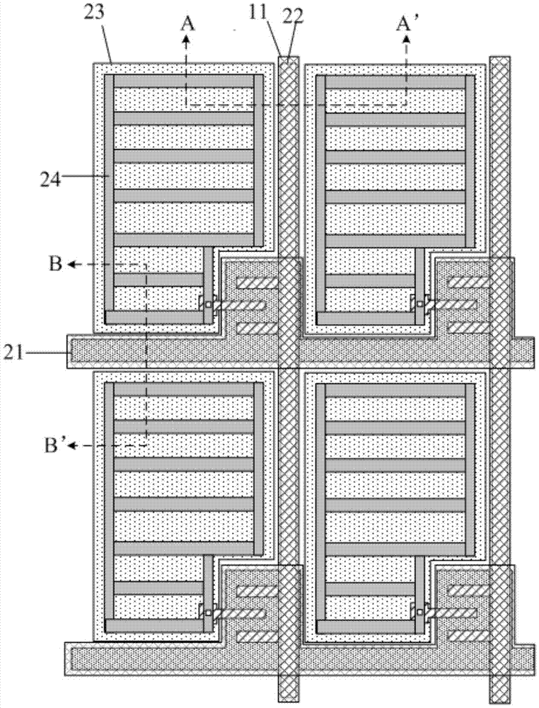
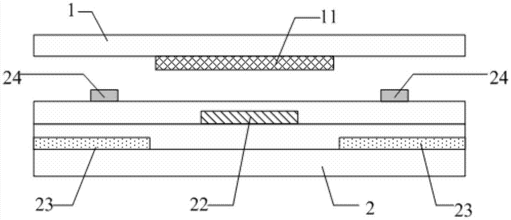
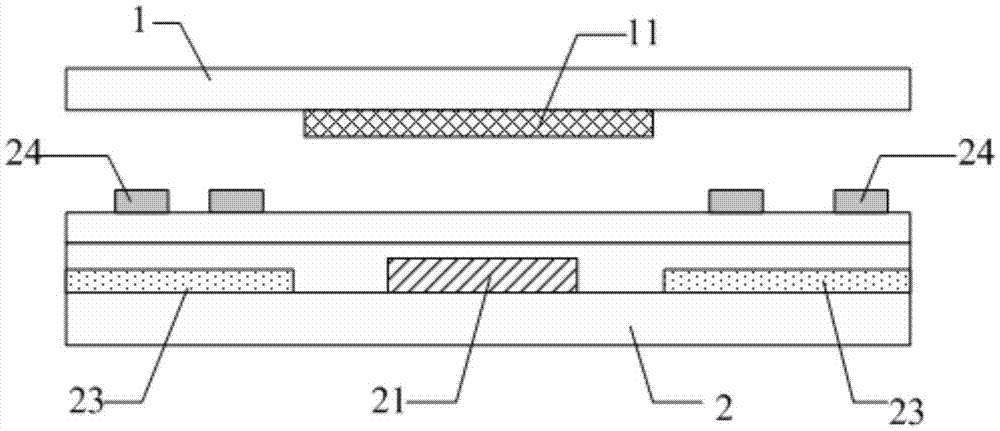
[0032] An array substrate 10 provided by an embodiment of the present invention, such as Figure 2a to Figure 2c As shown, it includes the base substrate 01, the gate line 02 located on the base substrate 01, and the common electrode 03 and the pixel electrode 04 which are sequentially located on the base substrate 01 and are insulated from each other, and the layer where the pixel electrode 04 is located is located on the gate l...


PUM


Abstract

The invention discloses an array substrate, a liquid crystal display panel and a display device. Due to the fact that a strip-shaped, transparent and conductive shielding electrode is arranged above a grid line, the outer profile of the projection, on a substrate, of the shielding electrode surrounds the projection, on the substrate, of the grid line, and the shielding electrode, pixel electrodes and the grid line are insulating to one another, so that the shielding electrode can shield an electric field above the grid line, even if the liquid crystal display panel formed by the array substrate generates displacement due to external force, deviation of liquid crystal is not affected, and the function of preventing light leakage can be achieved; besides, due to the fact that the shielding electrode can play the light leakage prevention role, in the liquid crystal display panel formed by the array substrate, a black matrix above the grid line can be omitted, and thus the aperture opening ratio and transmittance of the display panel are increased.

Description

technical field [0001] The invention relates to the field of display technology, in particular to an array substrate, a liquid crystal display panel and a display device. Background technique [0002] Liquid crystal displays have developed rapidly and have become mainstream flat panel displays. Since its appearance, liquid crystal displays have developed twisted nematic (TN) type, advanced ultra-dimensional field switch (Advanced DimensionSwitch, ADS) type, high aperture ratio and advanced ultra-dimensional field switch (High-Advanced DimensionSwitch, HADS) type and planar In-Plane Switch (In-PlaneSwitch, IPS) type and other types have different driving modes and display effects, and each has its own strengths. Among them, the ADS type and HADS type liquid crystal displays have shown excellent display capabilities and effects due to their unique structural characteristics and driving principles. [0003] The main difference between the ADS type and the HADS type liquid cry...

Claims


Application Information

Patent Timeline
Patent Type & Authority Applications(China)
IPC IPC(8): G02F1/1343
CPCG02F1/134309G02F1/13439G02F1/136209G02F2201/40G02F1/134372G02F1/133512G02F1/136218G02F1/136286
Inventor 肖文俊王世君陈希董学李治福姜文博薛艳娜李月包智颖吕振华张勇米磊耿越
Owner BOE TECH GRP CO LTD
Features
  • R&D
  • Intellectual Property
  • Life Sciences
  • Materials
  • Tech Scout
  • Unparalleled Data Quality
  • Higher Quality Content
  • 60% Fewer Hallucinations
Learn More