Array substrate structure and array substrate disconnection repair method

An array substrate structure and array substrate technology, applied in nonlinear optics, instruments, semiconductor devices, etc., can solve the problems of low repair efficiency, 300 long connection lines, and long time consumption, so as to improve the success rate of repair and facilitate broken line repair , the effect of reducing production costs

Active Publication Date: 2018-10-26
WUHAN CHINA STAR OPTOELECTRONICS TECH CO LTD
View PDF7 Cites 0 Cited by
  • Summary
  • Abstract
  • Description
  • Claims
  • Application Information

AI Technical Summary

Problems solved by technology

The disadvantage of this traditional repair method is that the connection line 300 is relatively long and the corresponding resistance is large; when the laser energy is high, it is easy to cause a short circuit between the connection line 300 and the gate scanning line 100 or the data line 200, and the repair success rate is low; And it takes a long time and the repair efficiency is low

Method used


Image

  • Array substrate structure and array substrate disconnection repair method
  • Array substrate structure and array substrate disconnection repair method
  • Array substrate structure and array substrate disconnection repair method

Examples


Embodiment Construction

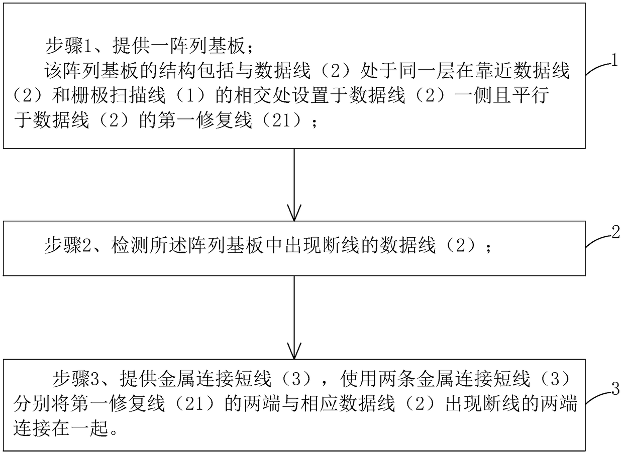
[0042] In order to further illustrate the technical means adopted by the present invention and its effects, the following describes in detail in conjunction with preferred embodiments of the present invention and accompanying drawings.

[0043] The invention provides an array substrate structure and an array substrate disconnection repair method.

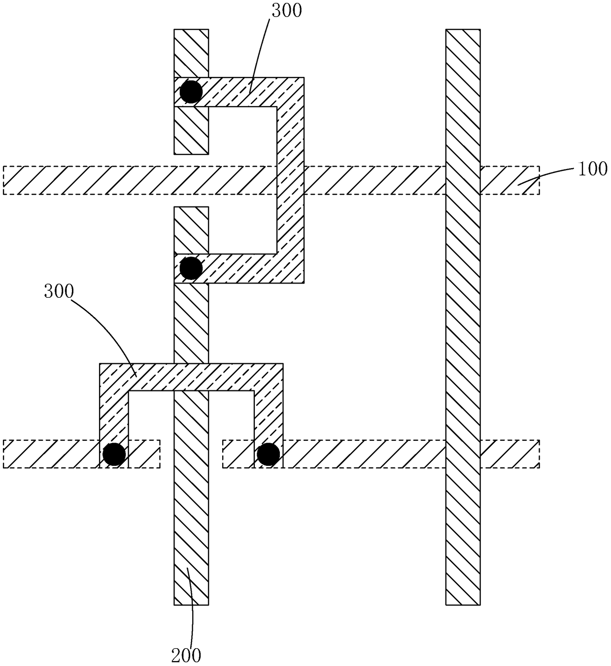
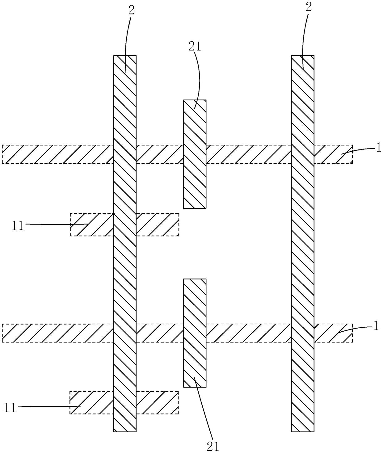
[0044] see figure 2 An array substrate structure provided by the present invention includes a plurality of parallel and spaced gate scanning lines 1, a plurality of mutually parallel spaced apart and vertically intersecting and insulated data lines 2 with the plurality of gate scanning lines 1 in space, In the same layer as the data line 2, the first repair line 21 arranged on the side of the data line 2 and parallel to the data line 2 at the intersection of the data line 2 and the gate scanning line 1, and the gate scanning line 1 is in the same layer and is arranged on the side of the gate scanning line 1 at the intersection of ...


PUM


Abstract

The invention provides an array substrate structure and an array substrate broken line repairing method. A first repair line (21) and a second repair line (22) which are located on the two sides of a data line (2) and parallel to the data line (2) are arranged near the position where the data line (2) intersects with a grid scanning line (1), a third repair line (11) and a fourth repair line (12) which are located on the two sides of the grid scanning line (1) and parallel to the grid scanning line (1) are arranged near the position where the data line (2) intersects with the grid scanning line (1), and the first repair line (21), the third repair line (11), the second repair line (22) and the fourth repair line (12) can be connected with the broken data line (2) or grid scanning line (1) through laser welding. In this way, broken line repair of an array substrate is facilitated, the repair success rate is increased, the repair process is simplified, repair efficiency is improved, and production cost is reduced.

Description

technical field [0001] The invention relates to the field of display technology, in particular to an array substrate structure and a method for repairing disconnection of the array substrate. Background technique [0002] Liquid Crystal Display (LCD) is widely used in mobile phones, TVs, personal digital assistants, digital cameras, notebook computers, desktop computers due to its advantages of high image quality, power saving, thin body and wide application range. Various consumer electronic products, such as LED display devices, have become the mainstream of display devices. [0003] Most of the liquid crystal displays currently on the market are backlight liquid crystal displays, which include a liquid crystal display panel and a backlight module (Backlight Module). The structure of the liquid crystal display panel is composed of a color filter substrate (Color Filter Substrate, CF Substrate), a thin film transistor array substrate (Thin Film Transistor Array Substrate, ...

Claims


Application Information

Patent Timeline
Patent Type & Authority Patents(China)
IPC IPC(8): G02F1/1362G02F1/13H01L27/12
CPCG02F1/1309G02F1/136259G02F1/136286G02F1/136263H01L27/1244
Inventor 杨祖有
Owner WUHAN CHINA STAR OPTOELECTRONICS TECH CO LTD
Why Eureka
Try Eureka