Defect detection device and method

A defect detection and line defect technology, applied in nonlinear optics, instruments, optics, etc., can solve the problems of invisible, unrepairable, large taper angle, etc., to improve accuracy, improve repair success rate, and improve product yield Effect

Active Publication Date: 2019-06-07
TCL CHINA STAR OPTOELECTRONICS TECH CO LTD
View PDF7 Cites 2 Cited by
  • Summary
  • Abstract
  • Description
  • Claims
  • Application Information

AI Technical Summary

Problems solved by technology

[0004] In the TFT-LCD industry, with the development of products to high resolution and shorter response time, a large number of copper processes are introduced into TFT array substrates to make metal wires. Due to the advantages of low resistance and high frequency of copper processes, aluminum materials have been replaced. It is widely used in large-size panels, but because the taper angle of the copper process is larger than that of aluminum, and due to the characteristics of the copper process (for example, the etchant is easy to over-etch the bottom of the metal wire), it is very easy to cause the metal wire to be undercut ( Undercut) line defects, which are invisible on the front side of the TFT array substrate, cannot be repaired, and are usually scrapped

Method used


Image

  • Defect detection device and method
  • Defect detection device and method
  • Defect detection device and method

Examples


Embodiment Construction

[0036] In order to further illustrate the technical means adopted by the present invention and its effects, the following describes in detail in conjunction with preferred embodiments of the present invention and accompanying drawings.

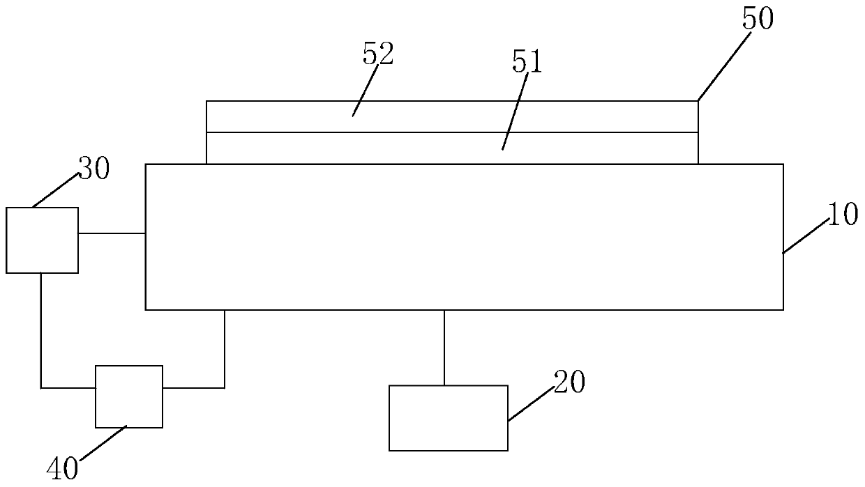
[0037] see figure 1, the present invention provides a defect detection device, comprising: a detection machine 10, a back camera unit 20 connected to the detection machine 10 and located below the detection machine 10, an array connected to the detection machine 10 A testing unit 30 and a processing unit 40 connected to the detection machine 10 and the array testing unit 30;

[0038] The back camera unit 20 is used to acquire an image of the back of the display panel 50;

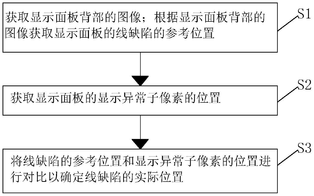
[0039] The detection machine 10 is used to obtain the reference position of the line defect of the display panel 50 according to the image on the back of the display panel 50;

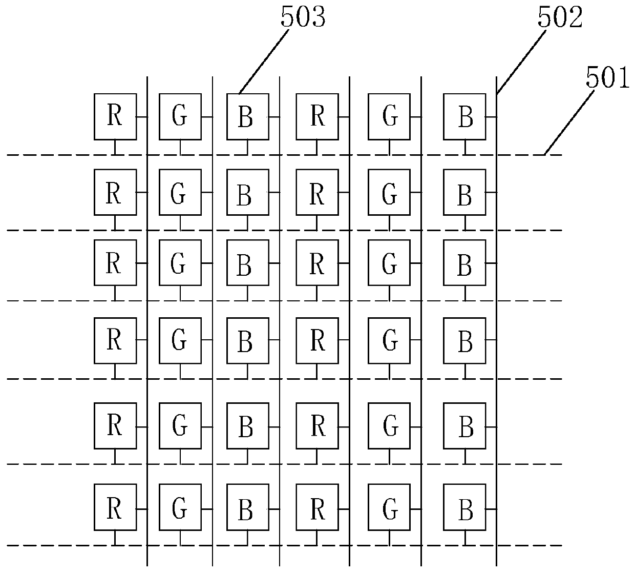
[0040] The array testing unit 30 is used to obtain the position of the sub-pixel displaying an ...


PUM


Abstract

The invention provides a defect detection device and method. The defect detection device comprises a detection machine table, a back camera shooting unit connected with the detection machine table andlocated below the detection machine table, an array testing unit connected with the detection machine table, and a processing unit connected with the detection machine table and the array testing unit; the back camera shooting unit is used for obtaining an image of the back of a display panel; the detection machine table is used for obtaining the reference position of a line defect of the displaypanel according to the image of the back of the display panel; the array testing unit is used for obtaining the position, displaying abnormal sub-pixels, of the display panel; and the processing unitis used for comparing the reference position of the line defect with the position displaying the abnormal sub-pixels so as to determine the actual position of the line defect. The positioning accuracy of the line defect is improved, thus the repairing success rate of the line defect is increased, and then the product yield is increased.

Description

technical field [0001] The invention relates to the field of display technology, in particular to a defect detection device and a defect detection method. Background technique [0002] Thin Film Transistor (TFT) is the main driving element in current Liquid Crystal Display (LCD) and Active Matrix Organic Light-Emitting Diode (AMOLED). It is related to the display performance of the flat panel display device. [0003] Most of the liquid crystal displays currently on the market are backlight liquid crystal displays, which include a liquid crystal display panel and a backlight module. The working principle of the liquid crystal display panel is to pour liquid crystal molecules between the thin film transistor array substrate (ThinFilm Transistor Array Substrate, TFT Array Substrate) and the color filter (ColorFilter, CF) substrate, and apply pixel voltage on the two substrates respectively. and the common voltage, through the electric field formed between the pixel voltage an...

Claims


Application Information

Patent Timeline
Patent Type & Authority Applications(China)
IPC IPC(8): G02F1/1362G02F1/13
Inventor 何伟
Owner TCL CHINA STAR OPTOELECTRONICS TECH CO LTD
Why Eureka
Try Eureka