High Gain Vertical Cavity Surface Emitting Semiconductor Laser Suitable for High Temperature Operation
A vertical cavity surface emission, high-gain technology, applied in the field of optoelectronics, can solve the problems of gain attenuation in the light-emitting area, and achieve the effects of simple preparation process, broad application prospects and wide application range.
- Summary
- Abstract
- Description
- Claims
- Application Information
AI Technical Summary
Problems solved by technology
Method used
Image

Examples
Embodiment Construction
[0026] The present invention will be described in further detail below in conjunction with the accompanying drawings and specific embodiments.
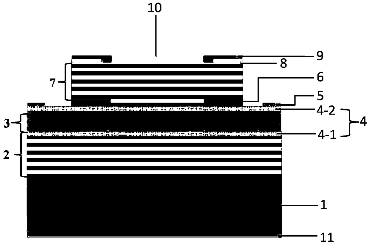
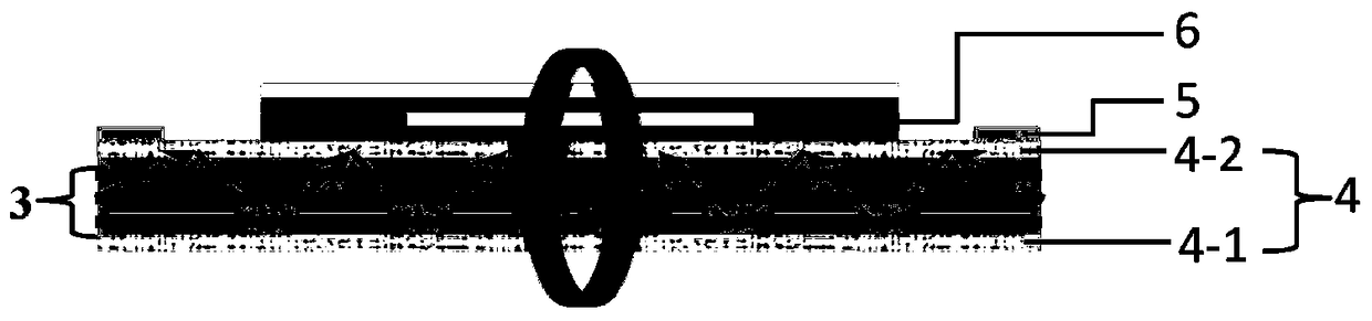
[0027] Such as figure 1 As shown, the high-gain vertical cavity surface-emitting semiconductor laser suitable for high-temperature operation has a structure from bottom to top: N-face electrode 11, N-type substrate 1, N-type doped DBR 2, active region 3, and gain guiding layer 4. Gain control electrode 5 , oxide layer 6 , P-type doped DBR 7 , P-side cover layer 8 and P-side electrode 9 , and the middle of P-side electrode 9 is a light exit window 10 . The gain guiding layer 4 is composed of an N-side gain guiding layer 4-1 and a P-side gain guiding layer 4-2, and is respectively located on the upper and lower sides of the active region 3; the gain control electrode 5 is located on the P side Gain guide layer 4-2, and the two are electrically connected.
[0028] When the laser is working, the gain control electrode 5 injects current ...
PUM
 Abstract
Description
Claims
Application Information
 - R&D
- Intellectual Property
- Life Sciences
- Materials
- Tech Scout
- Unparalleled Data Quality
- Higher Quality Content
- 60% Fewer Hallucinations
Browse by: Latest US Patents, China's latest patents, Technical Efficacy Thesaurus, Application Domain, Technology Topic, Popular Technical Reports.
© 2025 PatSnap. All rights reserved.Legal|Privacy policy|Modern Slavery Act Transparency Statement|Sitemap|About US| Contact US: help@patsnap.com