

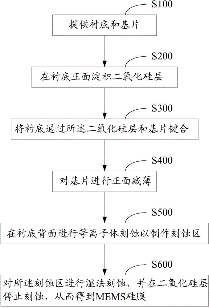
Production method for MEMS silicon film
A manufacturing method and technology of silicon film, which is applied in the direction of manufacturing tools, manufacturing microstructure devices, and photolithography on patterned surfaces, etc., can solve the problem of increasing device space, inaccurate size and thickness of silicon film, and difficulty in obtaining accurate thickness and size Silicon film and other issues
- Summary
- Abstract
- Description
- Claims
- Application Information
AI Technical Summary
Problems solved by technology
Method used
Image

Examples
Embodiment Construction
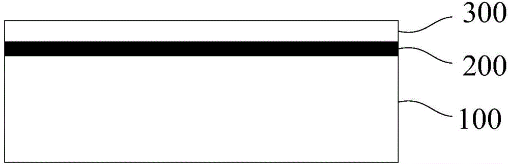
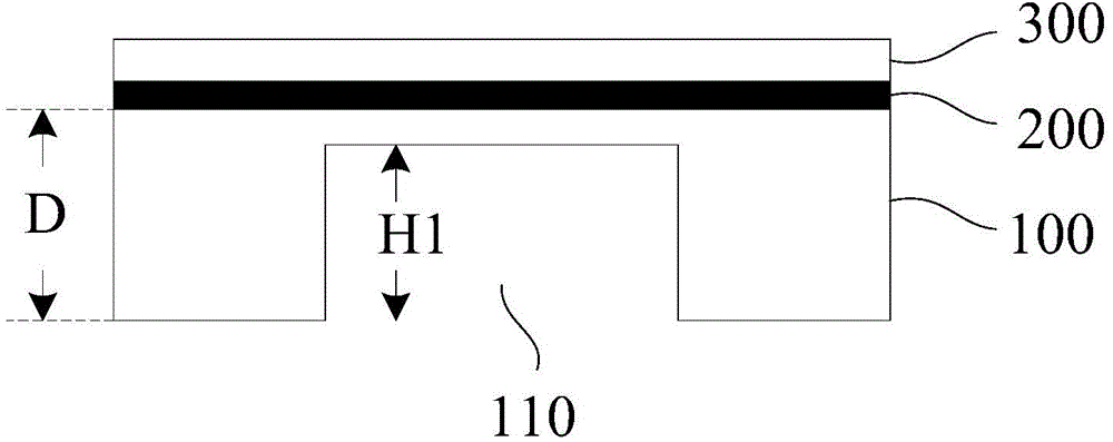
[0027] In order to facilitate the understanding of the present invention, the present invention will be described more fully below with reference to the associated drawings. Preferred embodiments of the invention are shown in the accompanying drawings. However, the present invention can be embodied in many different forms and is not limited to the embodiments described herein. On the contrary, these embodiments are provided to make the understanding of the disclosure of the present invention more thorough and comprehensive.
[0028] Unless otherwise defined, all technical and scientific terms used herein have the same meaning as commonly understood by one of ordinary skill in the technical field of the invention. The terms used herein in the description of the present invention are for the purpose of describing specific embodiments only, and are not intended to limit the present invention. As used herein, the term "and / or" includes any and all combinations of one or more of ...
PUM
| Property | Measurement | Unit |
|---|---|---|
| thickness | aaaaa | aaaaa |
Abstract
Description
Claims
Application Information