A semiconductor cooling device for high vacuum environment

A cooling device, semiconductor technology, applied in semiconductor/solid-state device manufacturing, electrical components, circuits, etc., to avoid uneven cooling and achieve the effect of cooling

Active Publication Date: 2018-07-03
SHENYANG SIASUN ROBOT & AUTOMATION
View PDF4 Cites 0 Cited by
  • Summary
  • Abstract
  • Description
  • Claims
  • Application Information

AI Technical Summary

Problems solved by technology

[0005] The invention aims to overcome the defects of the existing semiconductor cooling device, provide a semiconductor cooling device for high vacuum environment, and effectively realize the cooling of over-high temperature semiconductors

Method used


Image

  • A semiconductor cooling device for high vacuum environment
  • A semiconductor cooling device for high vacuum environment
  • A semiconductor cooling device for high vacuum environment

Examples


Embodiment Construction

[0025] In order to make the object, technical solution and advantages of the present invention clearer, the present invention will be further described in detail below in conjunction with the accompanying drawings and specific embodiments. It should be understood that the specific embodiments described here are only used to explain the present invention, but not to limit the present invention.

[0026] In the description of the present invention, the orientation or positional relationship indicated by the terms "inner", "outer", "longitudinal", "transverse", "upper", "lower", "top", "bottom" etc. are based on the drawings The orientations or positional relationships shown are only for the convenience of describing the invention and do not require the invention to be constructed and operated in a specific orientation, and thus should not be construed as limitations on the invention.

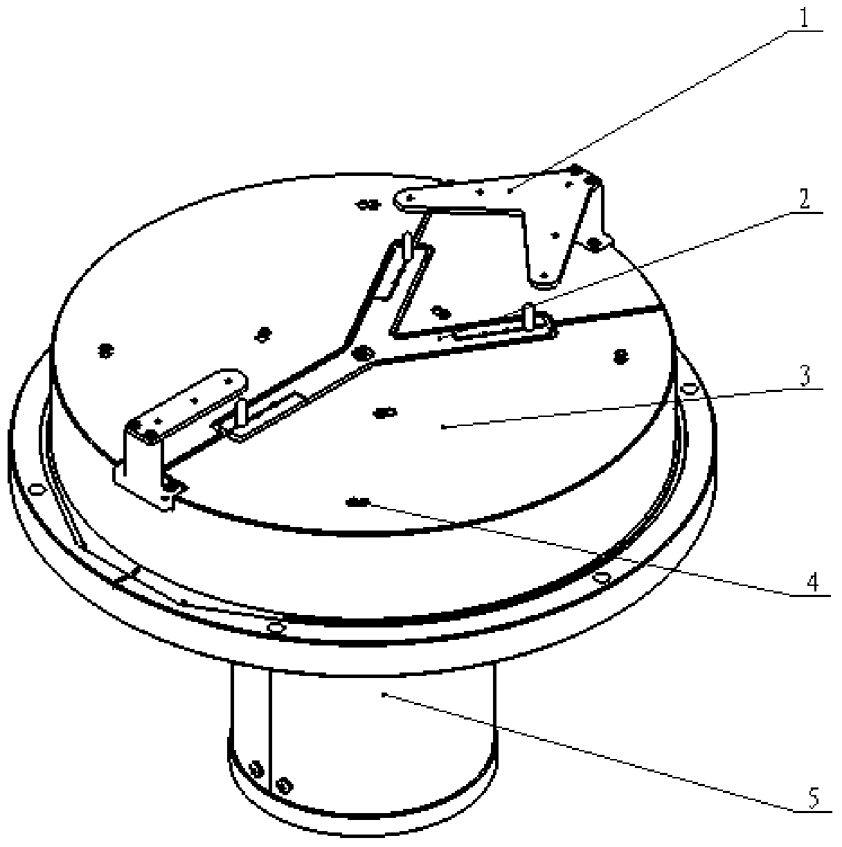
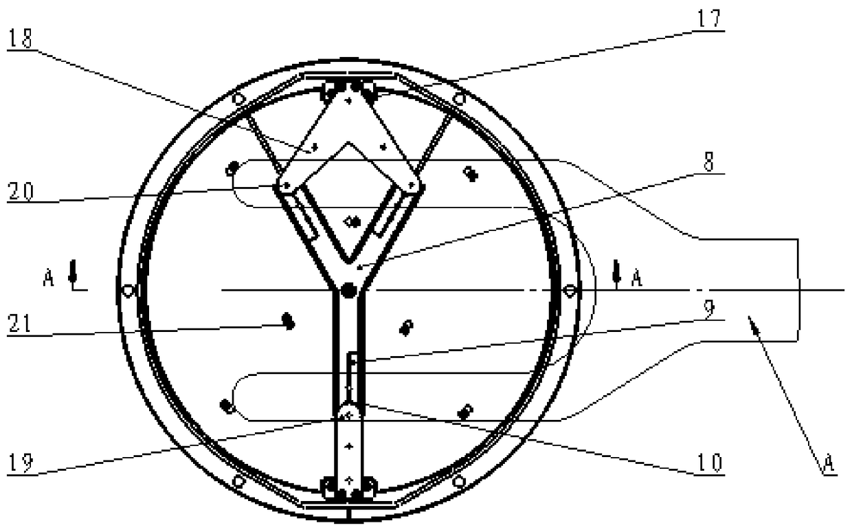
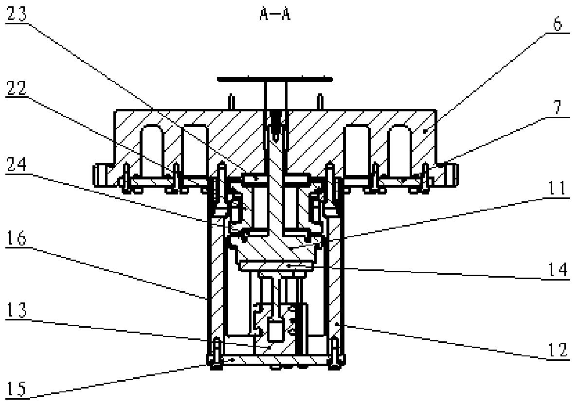
[0027] Such as figure 1 As shown, the present invention proposes a semiconductor cooling devi...


PUM


Abstract

The invention relates to the technical field of semiconductor processing, and specifically discloses a semiconductor cooling device used in a high vacuum environment. The semiconductor cooling device of the present invention comprises a wafer support mechanism (1), a lifting PIN support mechanism (2), a cooling plate mechanism (3), a cooling plate heat insulation support mechanism (4) and a pneumatic lifting mechanism (5), The wafer support mechanism (1), the lifting PIN support mechanism (2), and the cooling plate heat insulation support mechanism (4) are arranged on the cooling plate mechanism (3), and the cooling plate mechanism (3) is arranged on on the pneumatic lifting mechanism (5). The device of the invention realizes the automatic lifting function of the semiconductor and realizes the cooling of the semiconductor. Simultaneously, the invention aims at the realization of the cooling of the over-high temperature after semiconductor processing, and effectively realizes the cooling of the over-high temperature semiconductor.

Description

technical field [0001] The invention relates to the technical field of wafer processing, in particular to a semiconductor cooling device used in a high vacuum environment. Background technique [0002] At present, the growth rate of the global semiconductor consumption market and industry is very rapid, especially the growth rate of the domestic semiconductor consumption market and industry is more than 10 times that of the world. Under the extremely fierce competition in the semiconductor industry, the semiconductor industry increasingly needs extremely large-scale integration. [0003] Semiconductors integrate transportation, processing, and packaging. Due to the requirements of the processing technology, such as improving the production pass rate, the semiconductor will be heated at high temperature during the processing process. If the high-temperature semiconductor is directly packaged, it will damage the semiconductor packaging box and even damage the semiconductor. ...

Claims


Application Information

Patent Timeline
Patent Type & Authority Patents(China)
IPC IPC(8): H01L21/67
Inventor 李学威管莉娜赵治国何书龙王文钊吴青海
Owner SHENYANG SIASUN ROBOT & AUTOMATION
Why Eureka
Try Eureka