Packaging structure and method of metal wafer level groove buried hole type surface acoustic filter chip

A filter chip, packaging structure technology, applied in the direction of semiconductor/solid-state device parts, semiconductor devices, electrical components, etc., can solve the problems of long process, high cost, large structure size, etc., and achieve the effect of simple process

Active Publication Date: 2018-10-09
JCET GROUP CO LTD
View PDF7 Cites 0 Cited by
  • Summary
  • Abstract
  • Description
  • Claims
  • Application Information

AI Technical Summary

Problems solved by technology

[0004] The existing packaging method of surface acoustic filter devices has a long process, high cost, and relatively large structural size. Under the current trend of electronic equipment becoming smaller and smaller, it is necessary to continuously reduce the size of electronic devices and the components used in them. Weight and Dimensions of Surface Acoustic Filter Devices

Method used


Image

  • Packaging structure and method of metal wafer level groove buried hole type surface acoustic filter chip
  • Packaging structure and method of metal wafer level groove buried hole type surface acoustic filter chip
  • Packaging structure and method of metal wafer level groove buried hole type surface acoustic filter chip

Examples


Embodiment Construction

[0048] The present invention will be further described in detail below in conjunction with the accompanying drawings and embodiments.

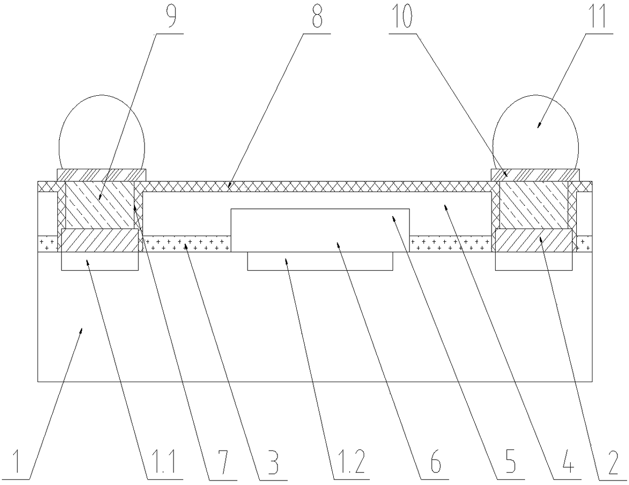
[0049] Such as figure 1 As shown, a metal wafer-level groove-buried surface surface acoustic filter chip packaging structure in this embodiment includes a surface acoustic filter chip wafer 1, and the surface of the surface acoustic filter chip wafer 1 includes an electrode area 1.1 and the sensing area 1.2, the surface of the electrode area 1.1 is provided with a first metal layer 2, the area of ​​the surface acoustic filter chip wafer 1 except the electrode area 1.1 and the sensing area 1.2 is provided with an adhesive glue 3, the adhesive A bonded wafer 4 is arranged above the glue 3, a cavity 6 is formed between the bonded wafer 4 and the sensing area 1.2, and a first opening 7 is provided at the position of the electrode area 1.1 of the bonded wafer 4, The surface of the bonded wafer 4 is provided with a first insulating layer 8, the fir...


PUM


Abstract

The invention relates to a metal-wafer-level groove buried hole type surface sound filtering chip packaging structure and method. The structure comprises a surface sound filtering chip wafer (1), wherein a first metal layer (2) is arranged on the surface of the surface sound filtering chip wafer (1); a laminated wafer (4) is arranged above the surface sound filtering chip wafer (1); a cavity (6) is formed between the laminated wafer (4) and the surface sound filtering chip wafer (1); a first open pore (7) is formed in the laminated wafer (4); a first insulating layer (8) is arranged on the surface of the laminated wafer (4); the first open pore (7) is filled with conductive adhesive or electroplated metal (9); a second metal layer (10) is arranged on the surface of the conductive adhesive or electroplated metal (9); and a corresponding metal ball (11) is arranged on the second metal layer (10). By adoption of the metal-wafer-level groove buried hole type surface sound filtering chip packaging structure and method provided by the invention, the surface sound filtering device with smaller area and volume, and lower manufacturing cost can be provided.

Description

technical field [0001] The invention relates to a packaging structure and method for a surface acoustic filter chip of a metal disc-level groove-buried hole type, and belongs to the technical field of semiconductor packaging. Background technique [0002] Surface acoustic filtering devices are widely used in RF and IF applications, including cellular phones, radiotelephones, and various radios. Through the use of surface acoustic filtering, these electronic devices are processed by filtering and delaying electrical signals. Due to the product performance and design functional requirements of the surface acoustic filter, it is necessary to ensure that the functional area of ​​the filter chip cannot touch any substance, that is, the cavity structure design. [0003] In the existing surface acoustic filter device packaging structure, the filter chip is connected to the ceramic substrate through conductive bump flip-chip welding and completely embedded in the cavity of the subs...

Claims


Application Information

Patent Timeline
Patent Type & Authority Patents(China)
IPC IPC(8): H01L23/31H01L23/48H01L23/52H01L21/50H01L21/60
CPCH01L21/50H01L23/31H01L23/48H01L23/52H01L24/02H01L24/80H01L2224/11
Inventor 张江华
Owner JCET GROUP CO LTD
Why Eureka
Try Eureka