A surface acoustic wave filter chip packaging structure

A chip packaging structure and surface acoustic wave filtering technology, applied in impedance networks, electrical components, etc., can solve the problems of thermal expansion of substrates, affecting the characteristics of electronic components, and brittleness of metal bumps and substrates. The effect of improving product reliability and improving manufacturing yield

Active Publication Date: 2021-12-24
JCET GROUP CO LTD
View PDF11 Cites 0 Cited by
  • Summary
  • Abstract
  • Description
  • Claims
  • Application Information

AI Technical Summary

Problems solved by technology

The existing surface acoustic wave filter uses metal bumps around the chip and the substrate to form a cavity by soldering, and the metal bumps and the substrate are connected by tin to form a rigid connection. However, the substrate has the problem of thermal expansion after being heated, and the generated heat Stress makes it difficult to control the warpage of the overall substrate, and the bonding surface between the metal bump and the substrate is prone to brittle fracture, which causes the packaging resin to flow into the gap between the substrate and the surface acoustic wave filter chip, contact the active area of ​​the chip, and affect the characteristics of electronic components

Method used


Image

  • A surface acoustic wave filter chip packaging structure
  • A surface acoustic wave filter chip packaging structure

Examples


Embodiment Construction

[0025] The present invention will be further described in detail below in conjunction with the accompanying drawings and embodiments.

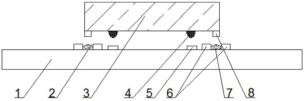
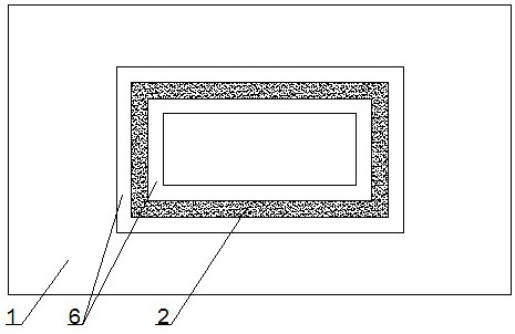
[0026] Such as figure 1 As shown, a surface acoustic wave filter chip packaging structure in this embodiment includes a substrate 1, a trench structure 2 is provided on the surface of the substrate 1, and the trench structure 2 is formed by a substrate circuit 6. Above the substrate 1 A chip 3 is provided, the bottom of the chip 3 is provided with a conductor 4, the chip 3 is electrically connected to the substrate circuit 5 through the conductor 4, a ring of bumps 8 is arranged around the bottom of the chip 3, and the bump 8 is located on the chip 3 the active area and the periphery of the conductor 4, the bump 8 fits with the trench structure 2, thereby forming a cavity structure in the active area of ​​the chip 3, and the periphery of the chip 3 and the trench structure 2 is encapsulated with a plastic encapsulant;

[0027] Further, the bu...


PUM


Abstract

The invention relates to a surface acoustic wave filter chip packaging structure, which includes a substrate (1), the surface of the substrate (1) is provided with a trench structure (2), and the trench structure (2) is formed by a substrate circuit (6), A chip (3) is arranged above the substrate (1), and a conductor (4) is arranged at the bottom of the chip (3), and the chip (3) is electrically connected to the circuit (5) of the substrate through the conductor (4). There is a ring of bumps (8) around the bottom of the chip (3), the bumps (8) are located in the active area of ​​the chip (3) and the periphery of the conductor (4), the bumps (8) and the trench structure (2) match, so that a cavity structure is formed in the active area of ​​the chip (3), and the periphery of the chip (3) and the trench structure (2) is encapsulated with plastic encapsulation compound. The present invention is a surface acoustic wave filter chip packaging structure, which effectively ensures the connection between the chip and the substrate through the fit design between the chip and the substrate, prevents the active area of ​​the chip from being polluted by the packaging resin, and can reduce the process steps and improve the manufacturing efficiency. yield.

Description

technical field [0001] The invention relates to a surface acoustic wave filter chip packaging structure, which belongs to the technical field of semiconductor packaging. Background technique [0002] The surface acoustic wave filter is based on the principle of sound waves, and a cavity needs to be provided in the packaging structure of the device. The existing surface acoustic wave filter uses metal bumps around the chip and the substrate to form a cavity by soldering, and the metal bumps and the substrate are connected by tin to form a rigid connection. However, the substrate has the problem of thermal expansion after being heated, and the generated heat Stress makes it difficult to control the warpage of the overall substrate, and the bonding surface between the metal bump and the substrate is prone to brittle fracture, which causes the packaging resin to flow into the gap between the substrate and the surface acoustic wave filter chip, contact the active area of ​​the ch...

Claims


Application Information

Patent Timeline
Patent Type & Authority Patents(China)
IPC IPC(8): H03H9/05H03H9/10
CPCH03H9/059H03H9/1064
Inventor 张超
Owner JCET GROUP CO LTD
Why Eureka
Try Eureka