Manufacturing method of metal wafer-level buried-hole type surface acoustic filter chip packaging structure

A filter chip and packaging structure technology, applied in semiconductor/solid-state device manufacturing, semiconductor/solid-state device components, semiconductor devices, etc., can solve the problems of long process, large structure size, high cost, etc., and achieve the effect of simple process

Active Publication Date: 2018-10-09
JCET GROUP CO LTD
View PDF4 Cites 0 Cited by
  • Summary
  • Abstract
  • Description
  • Claims
  • Application Information

AI Technical Summary

Problems solved by technology

[0004] The existing packaging method of surface acoustic filter devices has a long process, high cost, and relatively large structural size. Under the current trend of electronic equipment becoming smaller and smaller, it is necessary to continuously reduce the size of electronic devices and the components used in them. Weight and Dimensions of Surface Acoustic Filter Devices

Method used


Image

  • Manufacturing method of metal wafer-level buried-hole type surface acoustic filter chip packaging structure
  • Manufacturing method of metal wafer-level buried-hole type surface acoustic filter chip packaging structure
  • Manufacturing method of metal wafer-level buried-hole type surface acoustic filter chip packaging structure

Examples


Embodiment 1

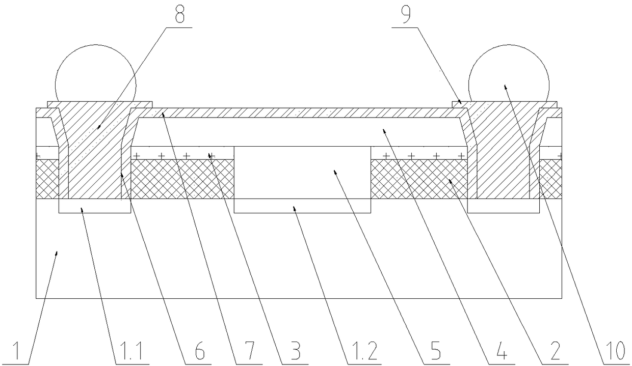
[0062] A method for manufacturing a package structure of a metal wafer-level buried-hole type surface acoustic filter chip, comprising the following process steps:

[0063] Step 1, see figure 2 , take a surface acoustic filter chip wafer;

[0064] Step 2. Prepare the first insulating layer

[0065] see image 3 1. Apply a certain thickness of insulating glue on the surface acoustic filter chip wafer by glue coating process, such as PI (polyimide), PA (nylon, polyamide), and use photolithography and development to seal the electrode area and Removal of the insulating glue at the sensing area of ​​the chip;

[0066] Step 3: Bonding wafer openings and bonding

[0067] see Figure 4 , take a piece of bonded wafer, first make a hole on the bonded wafer corresponding to the position above the electrode of the surface acoustic filter chip wafer, and then pass the bonding glue and surface acoustic filter through the bonded wafer that has been holed. Chip wafers are bonded toget...

Embodiment 2

[0082] A method for manufacturing a package structure of a metal wafer-level buried-hole type surface acoustic filter chip, comprising the following process steps:

[0083] Step 1, see Figure 10 , take a surface acoustic filter chip wafer;

[0084] Step 2. Prepare the first insulating layer

[0085] see Figure 11 1. Apply a certain thickness of insulating glue on the surface acoustic filter chip wafer by glue coating process, such as PI (polyimide), PA (nylon, polyamide), and use photolithography and development to seal the electrode area and Removal of the insulating glue at the sensing area of ​​the chip;

[0086] Step 3: Half-etch and bond the wafers and bond them

[0087] see Figure 12 , take a bonded wafer, first half-etch and open the bonded wafer corresponding to the position above the electrode of the surface acoustic filter chip wafer, and then connect the bonded wafer that has been half-etched to the surface through the adhesive The acoustic filter chip wafe...


PUM


Abstract

The invention relates to a manufacturing method for a metal disc buried-hole type surface acoustic filtering chip packaging structure. The method comprises the following steps of step 1, taking a surface acoustic filtering chip wafer; step 2, preparing a first insulating layer; step 3, forming an open hole in the wafer, and carrying out a wafer laminating step; step 4, preparing a second insulating layer; step 5, embedding the buried hole into the open hole through conductive adhesive or electroplating metal; step 6, preparing a second metal layer; step 7, carrying out reballing on the surface of the second metal layer; and step 8, cutting the obtained product into singe products. According to the manufacturing method for the metal disc buried-hole type surface acoustic filtering chip packaging structure, the surface acoustic filtering device with smaller area and size, and lower manufacturing cost is provided.

Description

technical field [0001] The invention relates to a method for manufacturing a package structure of a metal disc-level buried-hole type surface acoustic filter chip, and belongs to the technical field of semiconductor packaging. Background technique [0002] Surface acoustic filtering devices are widely used in RF and IF applications, including cellular phones, radiotelephones, and various radios. Through the use of surface acoustic filtering, these electronic devices are processed by filtering and delaying electrical signals. Due to the product performance and design functional requirements of the surface acoustic filter, it is necessary to ensure that the functional area of ​​the filter chip cannot touch any substance, that is, the cavity structure design. [0003] In the existing surface acoustic filter device packaging structure, the filter chip is connected to the ceramic substrate through conductive bump flip-chip welding and completely embedded in the cavity of the sub...

Claims


Application Information

Patent Timeline
Patent Type & Authority Patents(China)
IPC IPC(8): H01L21/56H01L23/31
CPCH01L21/561H01L23/3157H01L2224/11
Inventor 张江华
Owner JCET GROUP CO LTD
Why Eureka
Try Eureka