Heterogeneous phototransistors based on gesn‑gesi materials and their fabrication methods

A technology of phototransistor and manufacturing method, which is applied in the field of optoelectronics, can solve the problems of low light sensitivity and photocurrent, low light absorption coefficient, narrow detection range, etc., and achieve high light absorption efficiency, high absorption coefficient, high detection photocurrent and light sensitivity Effect

Inactive Publication Date: 2017-10-24
XIDIAN UNIV
View PDF4 Cites 0 Cited by
  • Summary
  • Abstract
  • Description
  • Claims
  • Application Information

AI Technical Summary

Problems solved by technology

The GeSn p-i-n type photodetector uses a new material of group IV GeSn with a narrower band gap and a higher light absorption coefficient, compared with the near-mid-infrared device of the III-V group material made in the prior art, it solves its difficult silicon-based The problem of integration can be compatible with the metal complementary oxide semiconductor CMOS (Complementary Metal Oxide Semiconductor) standard process; at the same time, compared with the shortcomings of the narrow detection range and low light absorption coefficient of Ge detectors used today, GeSn optoelectronics The detector has the advantages of wider detection wavelength and higher light absorption efficiency, but the GeSnp-i-n photodetector has the disadvantages of low light sensitivity and photocurrent
However, the disadvantages of this GeSn avalanche diode photodetector are that due to the fact that the noise is amplified and the additional noise generated during the multiplication process seriously interferes with the optical signal, and the bias voltage required for multiplication is extremely high. GeSn avalanche diode-type photodetectors are severely limited in practical applications

Method used


Image

  • Heterogeneous phototransistors based on gesn‑gesi materials and their fabrication methods
  • Heterogeneous phototransistors based on gesn‑gesi materials and their fabrication methods

Examples


Embodiment 1

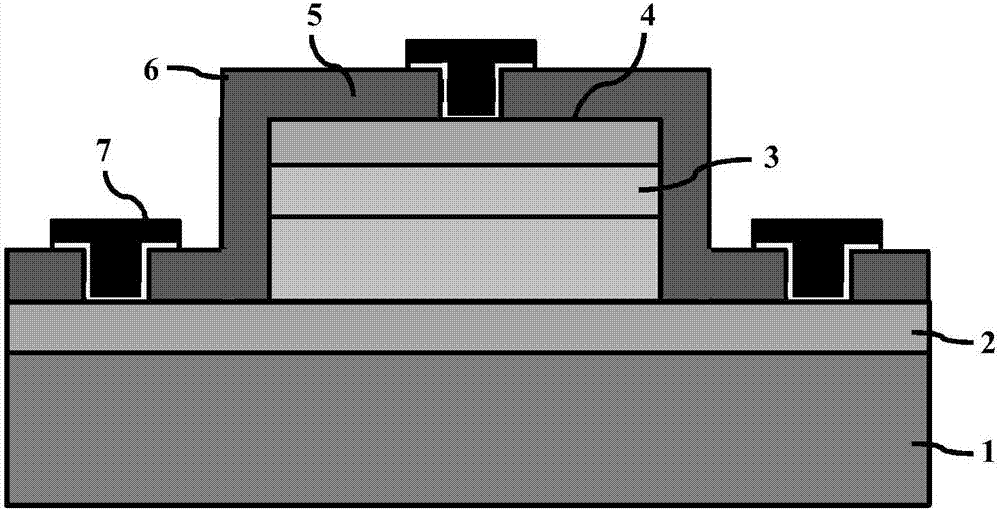
[0044] Embodiment 1: making Ge 0.935 sn 0.065 -Ge npn heterogeneous phototransistor and fabrication method thereof.

[0045] Step 1: Prepare a Ge layer.

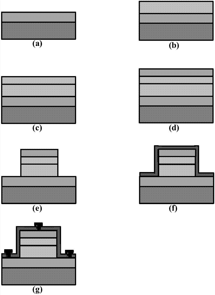
[0046] Using the low-temperature solid-source molecular beam epitaxy process, on the undoped (100) Ge substrate 1, at a temperature of 150°C, epitaxially grow an undoped pure Ge layer with a thickness of 800nm, such as figure 2 (a).

[0047] Step 2: Phosphorus ion implantation.

[0048] At an energy of 50KeV and an implant dose of 10 15 cm -2 , The implanted ions are P(31) under the condition that the substrate is tilted at an angle of 7° + Phosphorus ion implantation process to form Ge N + Type collector area 2.

[0049] Step 3: Prepare GeSn light absorption region.

[0050] Using low-temperature solid-source molecular beam epitaxy, the Ge N + Intrinsic Ge with a thickness of 100nm was epitaxially grown on the collector region at 150°C with high-purity Ge and Sn sources 0.935 sn 0.065 The epitaxial layer serves...

Embodiment 2

[0070] Embodiment 2: making Ge 0.97 sn 0.03 -Ge 0.9 Si 0.1 An npn heterogeneous phototransistor and a fabrication method thereof.

[0071] Step 1: Prepare GeSi.

[0072] Using the low-temperature solid-source molecular beam epitaxy process, epitaxially grow undoped Ge with a thickness of 800 nm on the undoped (100) Si substrate 1 at a temperature of 150 ° C. 0.9 Si 0.1 Floor.

[0073] Step 2: Phosphorus ion implantation.

[0074] At an energy of 50KeV and an implant dose of 10 15 cm -2 , The implanted ions are P(31) under the condition that the substrate is tilted at an angle of 7° + Phosphorus ion implantation process to form GeSiN + type collector area 2, such as figure 2 (a).

[0075] Step 3: preparing a GeSn light absorption region.

[0076] Using low-temperature solid-source molecular beam epitaxy, the GeSiN + Intrinsic Ge with a thickness of 100nm was epitaxially grown on the collector region at 150°C with high-purity Ge and Sn sources 0.97 sn 0.03 The e...

Embodiment 3

[0096] Embodiment 3: making Ge 0.9 sn 0.1 -Ge 0.6 Si 0.4 A pnp heterogeneous phototransistor and a fabrication method thereof.

[0097] Step A: preparing a GeSi layer.

[0098] Using the low-temperature solid-source molecular beam epitaxy process, epitaxially grow undoped Ge with a thickness of 800 nm on the undoped (100) Si substrate 1 at a temperature of 150 ° C. 0.6 Si 0.4 layer, such as figure 2 (a).

[0099] Step B: boron ion implantation.

[0100] At an energy of 50KeV and an implant dose of 10 15 cm -2 , The implanted ions are BF under the condition that the substrate is tilted at an angle of 7° 2 + boron ion implantation process to form GeSiP + Type collector area 2.

[0101] Step C: preparing a GeSn light absorption region.

[0102] Using low-temperature solid-source molecular beam epitaxy, the GeSiP + Intrinsic Ge with a thickness of 100nm was epitaxially grown on the collector region at 150°C with high-purity Ge and Sn sources 0.9 sn 0.1 The epitax...


PUM


Abstract

The invention discloses a GeSn-GeSi material based heterogeneous phototransistor and a fabrication method thereof. A collector and an emitter of the transistor both adopt a GeSi material, a light absorption region and a base region both adopt a GeSn material, an emitter region, the base region, the light absorption region and a collector region are sequentially and vertically arranged, and a passivation layer encircles the peripheries of the emitter region, the base region, the light absorption region and the collector region. According to the fabrication method of the transistor, the GeSn material is grown by a low-temperature solid-source molecular beam epitaxial process, and the fabrication method is a standard complementary metal oxide semiconductor (CMOS) fabrication method. The GeSn material with a high light absorption coefficient forms heterojunctions in the light absorption region, the GeSi emitter region and the collector region, the light sensitivity and light current during detection of an infrared light signal by the transistor are improved, and the GeSn-GeSi material based heterogeneous phototransistor has high light absorption rate.

Description

technical field [0001] The invention belongs to the field of optoelectronic technology, and further relates to a GeSn-GeSi material-based heterogeneous phototransistor and a manufacturing method thereof in the field of semiconductor infrared detection. The invention can detect near-middle-infrared light signals in the field of photoelectric near-middle-infrared detection. Background technique [0002] With the rapid development of integrated circuit technology and continuous advancement of technology, rapid processing and transmission of large-scale information data has become a bottleneck in the development of large-scale electronic devices today, and the effective integration of microelectronics technology and optoelectronics technology has become an effective way to solve this problem. [0003] Authors such as M Oehme disclosed a GeSn p-i-n type photodetector in their paper "GeSn-on-Si normal incidence photodetectors with bandwidths more than 40GHz" (Optics express, vol.2...

Claims


Application Information

Patent Timeline
Patent Type & Authority Patents(China)
IPC IPC(8): H01L31/028H01L31/0288H01L31/11H01L31/18
CPCH01L31/028H01L31/0288H01L31/1105H01L31/1812Y02P70/50
Inventor 韩根全王轶博张春福汪银花张进成郝跃
Owner XIDIAN UNIV
Why Eureka
Try Eureka