Photoelectric transistor based on GeSn materials and manufacturing method thereof

A technology of phototransistor and manufacturing method, applied in the field of electronics, can solve the problems of low light sensitivity and photocurrent, low light absorption coefficient, narrow detection range, etc., and achieve high light absorption efficiency, high absorption coefficient, high detection photocurrent and light sensitivity. Effect

Inactive Publication Date: 2016-10-12
XIDIAN UNIV
View PDF2 Cites 7 Cited by
  • Summary
  • Abstract
  • Description
  • Claims
  • Application Information

AI Technical Summary

Problems solved by technology

The GeSn p-i-n type photodetector uses a new material of group IV GeSn with a narrower band gap and a higher light absorption coefficient, compared with the near-mid-infrared device of the III-V group material made in the prior art, it solves its difficult silicon-based The problem of integration can be compatible with the metal complementary oxide semiconductor CMOS (Complementary Metal Oxide Semiconductor) standard process; at the same time, compared with the shortcomings of the narrow detection range and low light absorption coefficient of Ge detectors used today, GeSn optoelectronics The detector has the advantages of wider detection wavelength and higher light absorption efficiency, but the GeSn p-i-n photodetector has the disadvantages of low light sensitivity and photocurrent
Although the GeSn avalanche diode photodetector achieves higher light sensitivity and larger photocurrent by using the photoelectron multiplication method based on the advantages of the traditional GeSn photodetector, however, the GeSn avalanche diode photodetector has the disadvantages The disadvantage is that the GeSn avalanche diode photodetector is severely affected in practical applications due to the fact that the noise is amplified and the additional noise generated during the multiplication process seriously interferes with the optical signal, and the bias voltage required to achieve the multiplication is extremely high. limits

Method used


Image

  • Photoelectric transistor based on GeSn materials and manufacturing method thereof
  • Photoelectric transistor based on GeSn materials and manufacturing method thereof

Examples


Embodiment 1

[0036] Embodiment 1: making Ge 0.935 sn 0.065 npn type phototransistor.

[0037] Step 1: Growing the collector region.

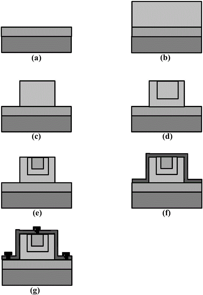
[0038] Using a low-temperature solid-source molecular beam epitaxy process, on an undoped (100) Ge substrate 1 at a temperature of 150° C., 200 nm of undoped pure Ge material is epitaxially grown as a Ge buffer layer.

[0039] On the Ge buffer layer, use high-purity Ge and Sn sources at 150°C to epitaxially generate 100nm Ge 0.935 sn 0.065 layer.

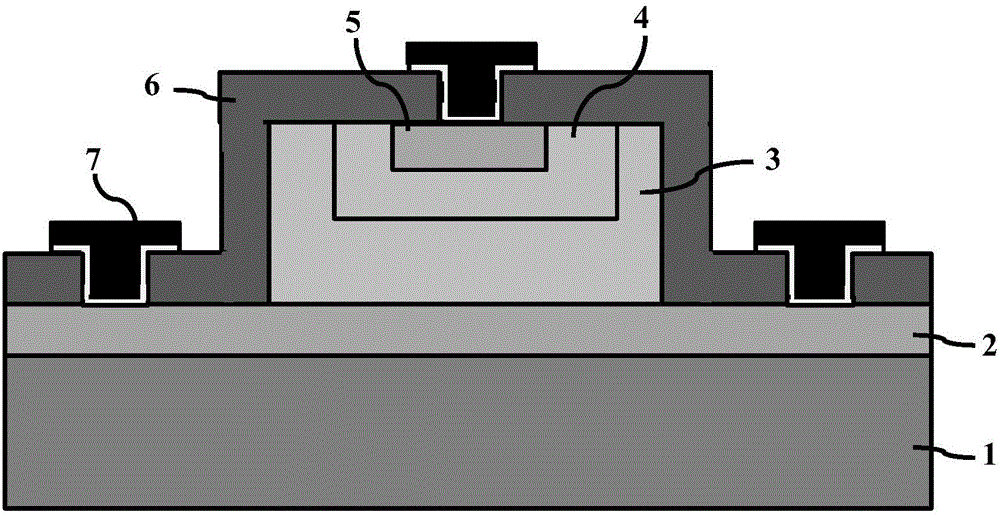
[0040]At an energy of 30Ke3V and an implant dose of 10 15 cm -2 , Implanting ions P(31) into the GeSn layer formed under the condition of a substrate tilt angle of 7° + , forming GeSn N + type collector area 2, such as figure 2 (a).

[0041] Step 2: Make the light absorbing area.

[0042] Using solid-source molecular beam epitaxy, the GeSn N + 220nm intrinsic Ge is grown on the collector region 2 at 150°C using high-purity Ge and Sn sources 0.935 sn 0.065 The epitaxial layer serves as the light abso...

Embodiment 2

[0053] Embodiment 2: making Ge 0.97 sn 0.03 pnp phototransistor

[0054] Step 1: growing the collector region.

[0055] Using the solid-source molecular beam epitaxy process, on the undoped (100) Si substrate 1 at a temperature of 150° C., a 200 nm undoped pure Ge material is epitaxially grown as a buffer layer.

[0056] Epitaxial Growth of 100nm Ge Using High Purity Ge and Sn Sources at 150℃ 0.97 sn 0.03 .

[0057] At an energy of 30KeV and an implant dose of 10 15 cm -2 , Implanting BF ions into the GeSn layer under the condition of a substrate tilt angle of 7° 2 + , forming GeSnP + type collector area 2, such as figure 2 (a).

[0058] Step 2: Make the light absorption area.

[0059] Using solid-source molecular beam epitaxy, the GeSnP + Epitaxial growth of 220nm intrinsic Ge on collector region 2 at 150°C 0.97 sn 0.03 The epitaxial layer serves as the GeSn light absorbing region 3, such as figure 2 (b).

[0060] Use reactive ion etching technology to etch...

Embodiment 3

[0070] Embodiment 3: making Ge 0.9 sn 0.1 npn phototransistor

[0071] Step A: Growing the collector region.

[0072] Using the solid-source molecular beam epitaxy process, on the undoped (100) Si substrate 1 at a temperature of 150° C., a 200 nm undoped pure Ge material is epitaxially grown as a buffer layer.

[0073] Epitaxial 100nm Ge on the buffer layer using the same conditions 0.9 sn 0.1 .

[0074] At an energy of 30KeV and an implant dose of 10 15 cm -2 , Implanting ions P(31) into the GeSn layer under the condition that the slice is tilted at an angle of 7° + Form GeSnN + type collector area 2, such as figure 2 (a).

[0075] Step B: Fabricate the light-absorbing region.

[0076] Using molecular beam epitaxy, the GeSn N + 220nm intrinsic Ge was grown on collector region 2 at 150°C 0.9 sn 0.1 The epitaxial layer serves as the light absorbing region 3, such as figure 2 (b).

[0077] Reactive ion etching technology is used to etch the desired pattern, suc...


PUM


Abstract

The invention discloses a photoelectric transistor based on GeSn materials and a manufacturing method thereof, aiming to solve the problem that present III-V infrared photodetectors are difficult to perform silicon-based integration and IV silicon and germanium detectors have a narrow detection range. The collector region, light absorption region, base region, and emitter region of the photoelectric transistor all employ IV GeSn alloys. A substrate, the collector region, the light absorption region, the base region, and the emitter region are successively vertically distributed, and a protective layer covers the periphery of the collector region, the light absorption region, the base region, and the emitter region. The photoelectric transistor is prepared by employing the standard CMOS (Complementary Metal Oxide Semiconductor) technique, utilizes GeSn materials having gaps and a high optical absorption coefficient, and has a wider infrared detection range compared with a Ge detector, and higher luminous sensitivity and photoelectric current.

Description

technical field [0001] The invention belongs to the field of electronic technology, and further relates to a phototransistor of GeSn material and a manufacturing method thereof in the field of semiconductor photoelectric technology. The invention can detect near-middle-infrared light signals in the field of photoelectric near-middle-infrared detection. Background technique [0002] With the rapid development of integrated circuit technology and continuous advancement of technology, rapid processing and transmission of large-scale information data has become a bottleneck in the development of large-scale electronic devices today, and the effective integration of microelectronics technology and optoelectronics technology has become an effective way to solve this problem. [0003] In their paper "GeSn-on-Si normal incidence photodetectors with bandwidths more than 40GHz" (Optics express, vol.22, pp.839-846, 2014), authors such as M Oehme disclosed a GeSn p-i-n type photodetecto...

Claims


Application Information

Patent Timeline
Patent Type & Authority Applications(China)
IPC IPC(8): H01L31/028H01L31/18
CPCH01L31/028H01L31/1812Y02P70/50
Inventor 韩根全王轶博张春福汪银花张进成郝跃
Owner XIDIAN UNIV
Why Eureka
Try Eureka