Liquid crystal display panel, manufacturing method thereof and display apparatus

A technology for liquid crystal display panels and manufacturing methods, applied to optics, instruments, electrical components, etc., capable of solving problems such as flickering and abnormal color of liquid crystal display panels

Inactive Publication Date: 2016-09-21
BOE TECH GRP CO LTD +1
View PDF5 Cites 22 Cited by
  • Summary
  • Abstract
  • Description
  • Claims
  • Application Information

AI Technical Summary

Problems solved by technology

Thus, the liquid crystal display panel can prevent the interference to the liquid crystal arrangement caused by the electrification of the black matrix pattern, an

Method used


Image

  • Liquid crystal display panel, manufacturing method thereof and display apparatus
  • Liquid crystal display panel, manufacturing method thereof and display apparatus
  • Liquid crystal display panel, manufacturing method thereof and display apparatus

Examples


Embodiment 1

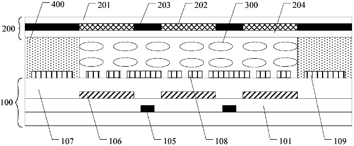
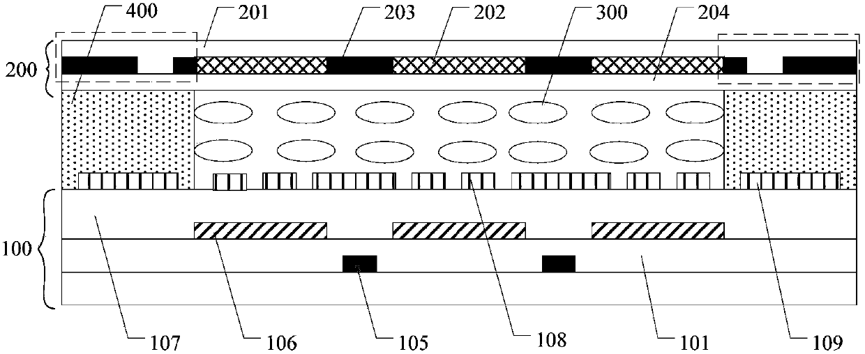
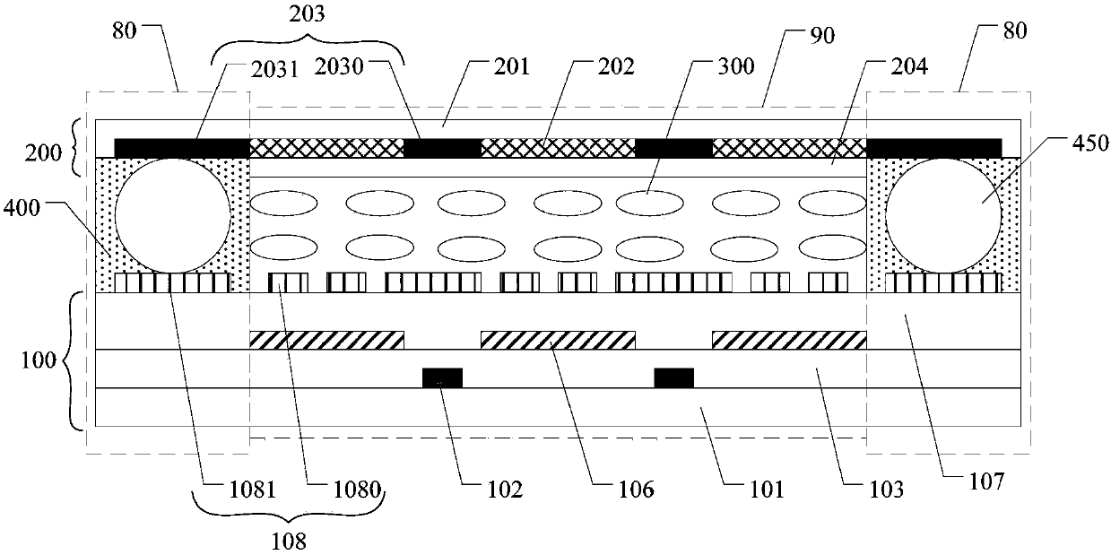
[0038] This embodiment provides a liquid crystal display panel, such as image 3 As shown, the liquid crystal display panel includes an array substrate 100, the array substrate 100 includes a first base substrate 101 and a common electrode pattern 108 disposed on the first base substrate 101; and an opposite substrate 200, the opposite substrate 200 includes a second The second base substrate 201 and the black matrix pattern 203 disposed on the second base substrate 201 . The array substrate 100 is disposed opposite to the opposite substrate 200 , and the common electrode pattern 108 is electrically connected to the black matrix pattern 203 .

[0039] In the liquid crystal display panel provided in this embodiment, the common electrode pattern 108 is electrically connected to the black matrix pattern 203 , therefore, the potential carried by the black matrix pattern 203 and the common electrode pattern 108 are the same. That is, when the common electrode pattern 108 is applie...

Embodiment 2

[0054] This embodiment provides a method for manufacturing a liquid crystal display panel, such as Figure 5 As shown, the manufacturing method includes the following steps S201-S203.

[0055] Step S201: providing an array substrate, the array substrate includes a first base substrate and a common electrode pattern disposed on the first base substrate.

[0056] Step S202: providing a counter substrate, the counter substrate includes a second base substrate and a black matrix pattern disposed on the second base substrate.

[0057] Step S203: aligning the array substrate and the opposite substrate, and electrically connecting the common electrode pattern and the black matrix pattern.

[0058]In the manufacturing method of the liquid crystal display panel provided in this embodiment, the common electrode pattern and the black matrix pattern are electrically connected, so the electric potential carried by the black matrix pattern and the common electrode pattern are the same. Th...

Embodiment 3

[0067] This embodiment provides a display device, which includes the liquid crystal display panel described in any one of the implementations. Therefore, the display device includes a technical effect corresponding to the technical effect of the liquid crystal display panel in the first embodiment, and its specific description can refer to the relevant description in the first embodiment, and will not be repeated here.

[0068] The display device provided by the embodiments of the present invention may be any product or component with a display function, such as electronic paper, a display, a mobile phone, a tablet computer, a television, a notebook computer, a digital photo frame, and a navigator.

[0069] The following points need to be explained:

[0070] (1) Embodiments of the present invention In the drawings, only the structures related to the embodiments of the present invention are involved, and other structures may refer to common designs.

[0071] (2) For clarity, i...


PUM


Abstract

The invention relates to a liquid crystal display panel, a manufacturing method of the liquid crystal display panel and a display apparatus. The liquid crystal display panel comprises an array substrate and an opposed substrate which is arranged opposite to the array substrate, wherein the array substrate comprises a first underlayer substrate and a common electrode pattern arranged on the first underlayer substrate, the opposed substrate comprises a second underlayer substrate and a black matrix pattern arranged on the second underlayer substrate, and the common electrode pattern is electrically connected with the black matrix pattern. By adopting the liquid crystal display panel, the interference on the alignment of liquid crystals caused by the electrification of the black matrix pattern can be prevented, and the problem that the liquid crystal display panel is abnormal in picture color or flashes due to the electrification of the black matrix pattern can be solved.

Description

technical field [0001] Embodiments of the present invention relate to a liquid crystal display panel, a manufacturing method of the liquid crystal display panel, and a display device. Background technique [0002] With the continuous development of the display device market, Liquid Crystal Display (LCD) has become a mainstream display device due to its advantages of fast response, high integration, and low power consumption. A liquid crystal display panel generally includes a liquid crystal cell formed by an array substrate including a thin film transistor (Thin Film Transistor, TFT) and an opposite substrate arranged opposite to the cell, and a layer of liquid crystal molecules filled in the liquid crystal cell. [0003] Black matrix is ​​an important part of LCD. The basic function of the black matrix is ​​light shading, the purpose is to improve contrast, avoid color mixing of adjacent sub-pixels, reduce external light reflection and prevent leakage current caused by ext...

Claims


Application Information

Patent Timeline
IPC IPC(8): G02F1/1335G02F1/1343G02F1/1333
CPCG02F1/1333G02F1/133512G02F1/134309G02F1/134363G02F2202/16G02F1/136204G02F1/133354G02F1/136218G02F1/1345G02F2202/22G02F1/1339H01L23/60
Inventor 黄式强
Owner BOE TECH GRP CO LTD
Why Eureka
Try Eureka