Wiring method of superconducting quantum bit system for surface coding scheme and wiring board

A technology of superconducting quantum and quantum bits, applied in the field of quantum systems, can solve the problems of reduced decoherence time and inability to work of quantum bits

Active Publication Date: 2016-09-21
INST OF PHYSICS - CHINESE ACAD OF SCI
View PDF3 Cites 24 Cited by
  • Summary
  • Abstract
  • Description
  • Claims
  • Application Information

AI Technical Summary

Problems solved by technology

However, the qubit system is extremely fragile, and the insulating layer covered on the qubit may cause the decoherence time of the qubit to be greatly reduced, eventually causing it to fail to work

Method used


Image

  • Wiring method of superconducting quantum bit system for surface coding scheme and wiring board
  • Wiring method of superconducting quantum bit system for surface coding scheme and wiring board

Examples


Embodiment 1

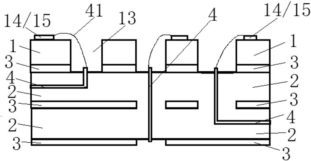
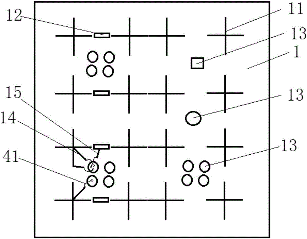
[0026] figure 1 It is a structural schematic diagram of a wiring board for a surface coding scheme superconducting qubit system according to an embodiment of the present invention, figure 2 It is a schematic top view of a wiring board used in a surface coding scheme superconducting qubit system according to an embodiment of the present invention. Such as figure 1 As shown, a wiring board for a superconducting qubit system of a surface coding scheme includes: a quantum chip substrate 1 , several insulating layers 2 , several grounding layers 3 and wiring layers 4 . Quantum chip substrate 1 is provided with several qubits 11 ( figure 2 shown) and several couplers 12 ( figure 2 shown), the several qubits 11 ( figure 2 shown) between any two adjacent qubits 11 directly coupled or through the several couplers 12 ( figure 2 Shown) in the corresponding coupler 12 coupling; Insulation layer 2 covers and is arranged on the lower surface of described quantum chip substrate 1; ...

Embodiment 2

[0031] The present invention also provides a wiring method for a superconducting qubit system of a surface coding scheme, which is applied to the wiring of a superconducting qubit system having a quantum chip substrate 1, an insulating layer 2, and a grounding layer 3 as described above The plate includes: wiring under the quantum chip substrate 1, punching a hole 13 on the quantum chip substrate 1, and connecting the wiring to the circuit on the quantum chip substrate 1 through the hole 13, The wiring forms the wiring layer 4 .

[0032] In a preferred embodiment, the wiring layer 4 is penetrated in the insulating layer 2 below the quantum chip substrate 1, and the insulating layer 3 pierced with the wiring layer 4 can be one or more layers; the wiring layer 4 can be set in the same insulating layer 2 or in different insulating layers 2 . Preferably, the upper surface and the lower surface of the insulating layer 2 are covered with a ground layer 3 made of metal. The metal m...


PUM


Abstract

The invention provides a wiring method of a superconducting quantum bit system for a surface coding scheme and a wiring board, and belongs to the field of a quantum system. The wiring board comprises a quantum chip substrate, a plurality of insulating layers, a wiring layer and a plurality of grounding layers, wherein the quantum chip substrate is provided with a plurality of quantum bits and a plurality of couplers, and the insulating layers are arranged at the lower surface of the quantum chip substrate in a covering manner; the wiring layer is arranged in the insulating layers of the plurality of insulating layers, and the wiring layer is connected with the quantum bits and / or the couplers; and the plurality of grounding layers are correspondingly arranged at the upper surfaces and the lower surfaces of the plurality of insulating layers. According to the wiring method provided by the invention of the superconducting quantum bit system for the surface coding scheme and the wiring board, a problem that the quantum bit de-coherence time is reduced because key devices such as the quantum bits are covered with an insulating film is avoided through the wiring board provided with the quantum chip substrate, the insulating layers and the grounding layers.

Description

technical field [0001] The invention relates to the field of quantum systems, in particular to a wiring method and a wiring board for a superconducting qubit system of a surface coding scheme. Background technique [0002] Quantum computing is superior to known classical computing algorithms in the speed of solving mathematical problems such as large prime number factorization and global search. People have realized some simple quantum algorithms in many different quantum systems, and the superconducting qubit system is one of the most promising systems. [0003] However, because the existing qubit system is extremely fragile, various noises in the environment will cause rapid decoherence of the qubit system, making it impossible to complete more complex quantum algorithms. In order to overcome this problem, on the one hand, people focus on improving the decoherence time of the qubit system; on the other hand, Shor et al. borrowed from the error correction coding scheme of ...

Claims


Application Information

Patent Timeline
Patent Type & Authority Applications(China)
IPC IPC(8): H01L21/768H01L23/485
CPCH01L21/768H01L23/485H01L2224/48091H01L2224/73265H01L2924/00014
Inventor 郑亚锐吴玉林邓辉郭学仪闫智广宁鲁慧金贻荣朱晓波郑东宁
Owner INST OF PHYSICS - CHINESE ACAD OF SCI
Why Eureka
Try Eureka