Micro light emitting diode array's transfer printing method

A technology of micro light-emitting diodes and arrays, which is applied in the manufacture of semiconductor devices, electrical components, semiconductor/solid-state devices, etc., and can solve problems such as inability to adapt to pattern structures.

Active Publication Date: 2016-10-26
SHENZHEN CHINA STAR OPTOELECTRONICS TECH CO LTD
View PDF4 Cites 55 Cited by
  • Summary
  • Abstract
  • Description
  • Claims
  • Application Information

AI Technical Summary

Problems solved by technology

Then when using a PDMS-type transfer head to transfer Micro LEDs, since the adhesion of the PDMS film layer is similar ever

Method used


Image

  • Micro light emitting diode array's transfer printing method
  • Micro light emitting diode array's transfer printing method
  • Micro light emitting diode array's transfer printing method

Examples


Embodiment Construction

[0026] In order to further illustrate the technical means adopted by the present invention and its effects, the following describes in detail in conjunction with preferred embodiments of the present invention and accompanying drawings.

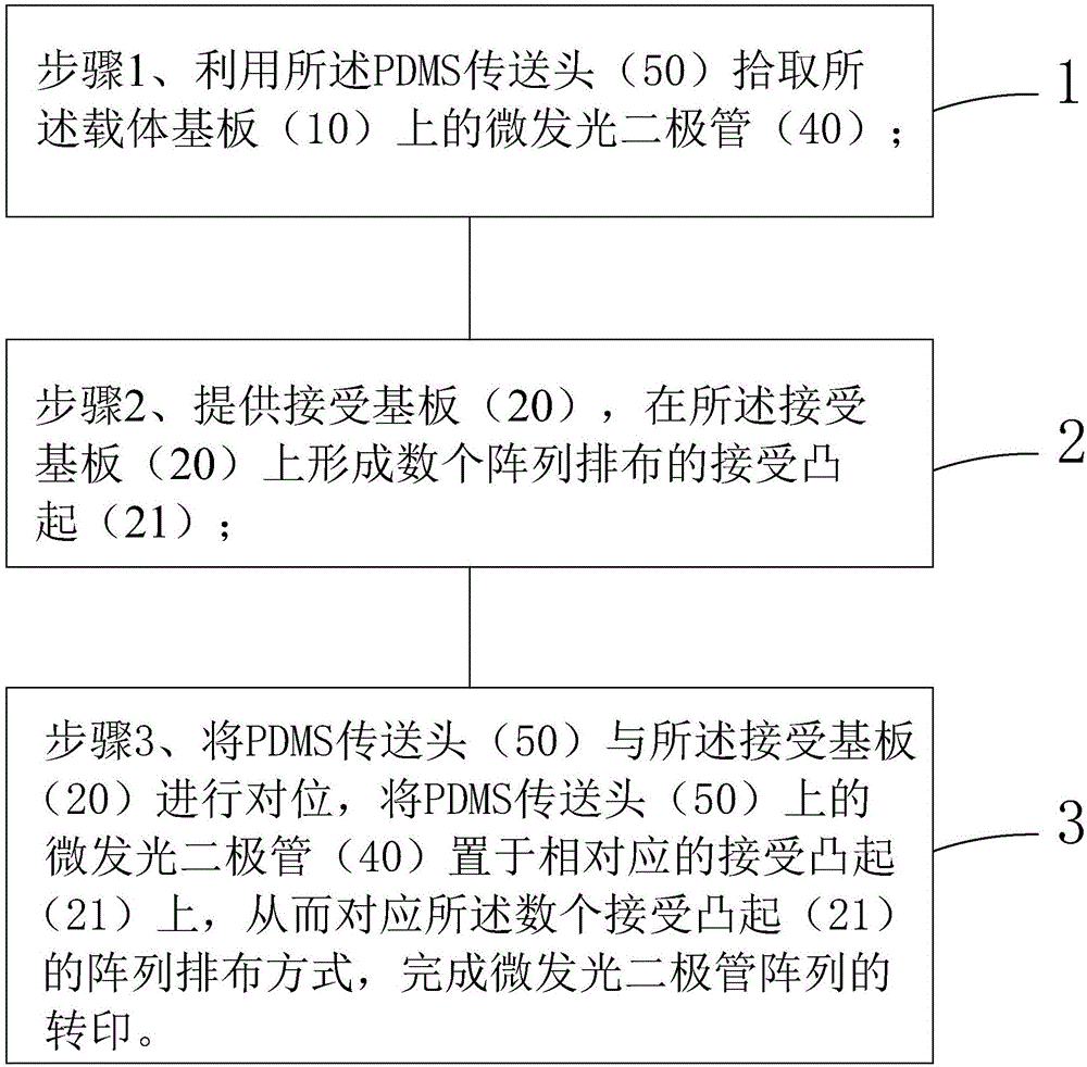
[0027] see figure 1 , the present invention provides a transfer printing method of a micro light emitting diode array, comprising the following steps:

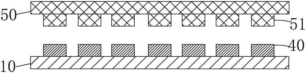
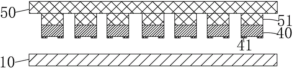
[0028] Step 1, such as Figure 2-3 As shown, a transfer head 50 and a carrier substrate 10 are provided, on which several micro LEDs 40 are arranged, and the transfer head 50 is used to pick up the micro LEDs 40 on the carrier substrate 10 .

[0029] Specifically, the transfer head 50 may be a PDMS transfer head, including a PDMS film layer, and the PDMS film layer has several raised structures 51 arranged in an array. In the step 1, the protrusions of the PDMS film layer are used The structure 51 picks up the micro light emitting diodes 40 through the adsorption force. In addition, the tra...


PUM

PropertyMeasurementUnit
Heightaaaaaaaaaa

Abstract

The invention provides a micro light emitting diode array's transfer printing method. A plurality of projections are arranged on a receiving substrate; micro light emitting diodes are placed on the corresponding projections on the receiving substrate; therefore, for the same transfer head, the change in the arraying manner of a plurality of projections on the receiving substrate make possible the transfer printing of micro light emitting diode arrays in different arraying manners on a receiving substrate.

Description

technical field [0001] The invention relates to the field of display technology, in particular to a transfer printing method of a micro light emitting diode array. Background technique [0002] Micro LED (Micro LED) is a device with a size between several microns and hundreds of microns. Because it is much smaller than ordinary LEDs, it is possible to use a single LED as a pixel (Pixel) for display. A Micro LED display is a display that uses a high-density Micro LED array as a display pixel array to achieve image display. Like a large-scale outdoor LED display, each pixel can be addressed and individually driven to light up. It can be regarded as a A reduced version of the outdoor LED display, which reduces the pixel distance from millimeters to microns. Micro LED displays are self-luminous displays like Organic Light-Emitting Diode (OLED) displays, but Micro LED displays are compared to OLED displays also have the advantages of better material stability, longer life, and n...

Claims


Application Information

Patent Timeline
IPC IPC(8): H01L33/48H01L33/62H01L25/075H01L21/60
CPCH01L24/24H01L24/82H01L25/0753H01L33/486H01L33/62H01L2224/24226H01L2224/82895H01L2933/0066H01L2933/0033
Inventor 陈黎暄
Owner SHENZHEN CHINA STAR OPTOELECTRONICS TECH CO LTD
Why Eureka
Try Eureka