Packaging device for a light-transmitting carrier and an electroluminescent device

A technology of electroluminescent devices and packaging devices, which is applied to semiconductor devices, electrical components, circuits, etc., and can solve problems such as deformation of glass substrates or PET films

Active Publication Date: 2019-02-05
NANJING TECH CORP LTD
View PDF6 Cites 0 Cited by
  • Summary
  • Abstract
  • Description
  • Claims
  • Application Information

AI Technical Summary

Problems solved by technology

[0004] The purpose of the invention is to solve the problem of warping and deformation of the glass substrate or PET film during the heating and cooling process of the device manufacturing process, and to provide a light-transmitting carrier and a packaging device for the electroluminescent device, which can effectively prevent During the curing process of UV glue for electroluminescent devices, due to the warping and deformation of the glass or PET film substrate or cover plate during the process of heating and cooling in the process, the surface of the double-layer glass or double-layer PET film is smoother and improved. Cutting yield, IC bonding yield and product lifespan

Method used


Image

  • Packaging device for a light-transmitting carrier and an electroluminescent device
  • Packaging device for a light-transmitting carrier and an electroluminescent device
  • Packaging device for a light-transmitting carrier and an electroluminescent device

Examples


Embodiment 1

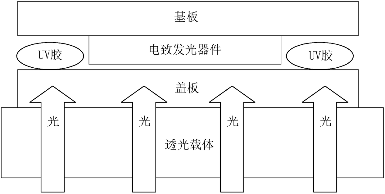
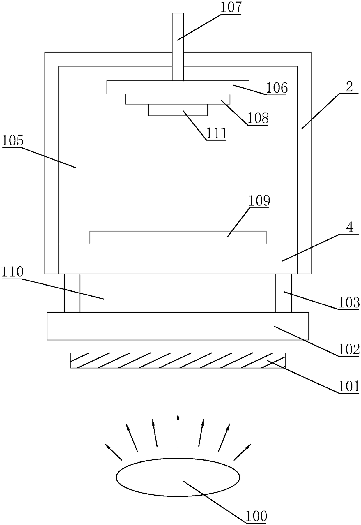
[0043] like figure 2 A packaging device for an electroluminescent device is shown, including a light source 100, a cover part 2, an adsorption tool 106, a heat insulation component 110, a second light-transmitting plane carrier 102, a transport mechanism 107 for driving the adsorption tool 106, and negative pressure adsorption The light-transmitting carrier 4 is formed between the cover part 2 and the light-transmitting carrier 4 to form a sealed space 105 for packaging the electroluminescent device.

[0044] The movable cover part 2 is used to open and close the sealed space 105 of the packaging device, and the transportation mechanism 107 drives the suction tool 106 to move the electroluminescent device to the suction surface of the transparent carrier 4 for packaging and suction correction.

[0045] The cover part 2 is provided with a pressure regulating port, and the air pressure in the sealed space 105 is adjusted by connecting a negative pressure device (which can be a co...

Embodiment 2

[0070] Compared with Embodiment 1, this embodiment differs in that: the structure of negative pressure voids of the light-transmitting carrier 4 is different.

[0071] like Figure 7 to Figure 9 As shown, the negative pressure gaps on the surface of the transparent carrier 4 in this embodiment are grooves 42 , and the grooves 42 are distributed in a closed ring along the outer periphery of the transparent carrier. The negative pressure port 40 communicates with the grooves 42 through the airflow channel 41 .

[0072] Similarly, the groove 42 is also distributed in the non-display area of ​​the light-transmitting carrier 4. The groove 42 can be single or multiple. The groove in this embodiment is an annular groove 42, and along the non-display Arranging the inner and outer periphery of the area can meet the basic needs of adsorption correction.

[0073] By extracting air from the negative pressure interface 40 , a negative pressure is generated in the entire annular groove 42 ...

Embodiment 3

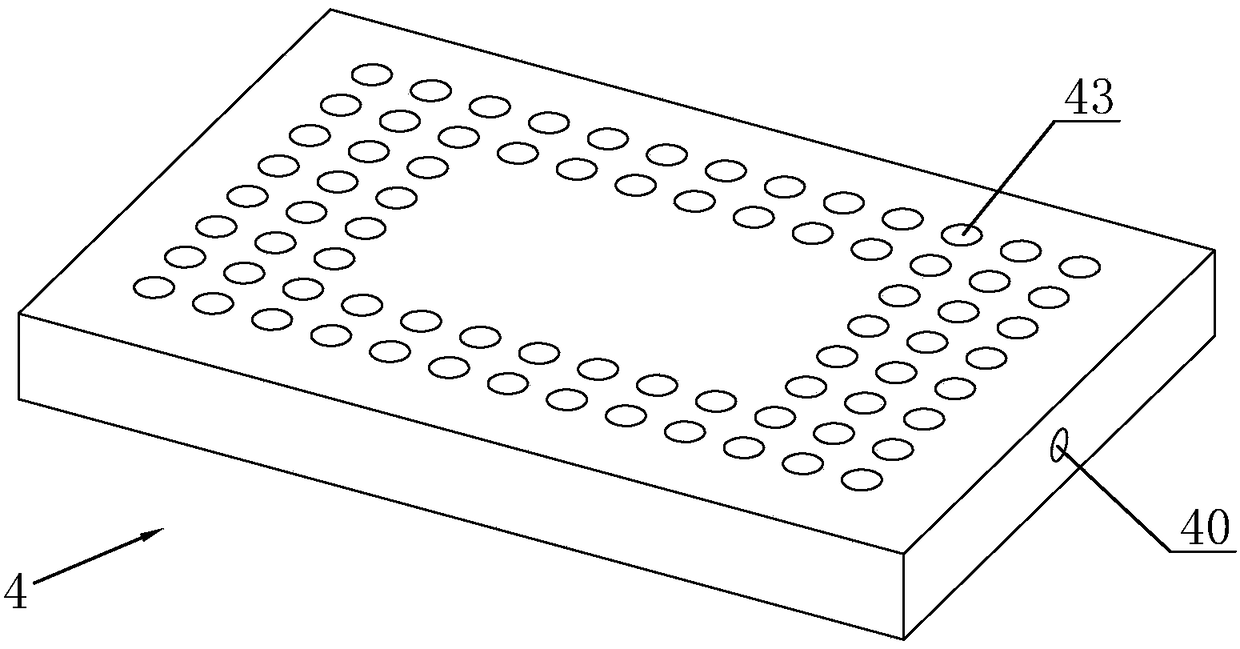
[0078] like Figure 10 and Figure 11 As shown, this embodiment is a combination of Embodiment 1 and Embodiment 2. The adsorption surface of the light-transmitting carrier 4 has both an annular groove 42 and a negative pressure through hole 43, wherein the groove 42 and the negative pressure through hole 43 are both In the non-display area of ​​the snap surface.

[0079] like Figure 10 As shown, the negative pressure through holes 43 are located in the groove 42. The groove 42 is in the shape of a square ring. in the non-display area.

[0080] Compared with the embodiment 1, the groove 42 has a better adsorption effect on the edge periphery of the cover plate in this embodiment, and the cover plate is not easy to fall off. Compared with the second embodiment, the negative pressure through hole 43 also makes up for the lack of adsorption inside the cover plate in this embodiment. It is equivalent to concentrating the advantages of Embodiment 1 and Embodiment 2.


PUM


Abstract

The invention discloses a light-transmittance carrier, and a packaging apparatus for an electroluminescent device. The packaging apparatus for the electroluminescent device comprises the light-transmittance carrier; the light-transmittance carrier comprises an adsorption surface which is used for being attached with an adsorption object, a negative pressure air gap which is used for being adsorbed with the adsorption object, and a negative pressure interface which is used for being connected with a negative pressure apparatus; the negative pressure interface is formed in the light-transmittance carrier; and the light-transmittance carrier also comprises an air flow channel which is used for being connected with the negative pressure air gap and the negative pressure interface. The light-transmittance carrier is matched with the adsorption effect of the negative pressure apparatus; the light-transmittance carrier is applied to the packaging apparatus for the electroluminescent device, so that the phenomena of edge warping and deformation of glass or a PET film substrate or a cover plate caused in the temperature rise and cooling processes in the craft process in the UV adhesive curing process of the electroluminescent device can be effectively avoided; and therefore, the surface of the dual-layer glass or the dual-layer PET film is more smooth, so that the cutting yield can be improved, the IC bonding yield can be increased, and the service life of the product can be prolonged.

Description

technical field [0001] The invention relates to the technical field of packaging of display devices, in particular to a packaging device for a light-transmitting carrier and an electroluminescent device. Background technique [0002] Generally, an electroluminescent device includes a substrate, a cover plate, and a light-emitting element arranged between the substrate and the cover plate. When the light-emitting element of an electroluminescent device is prepared, regardless of the evaporation method (when the reflective electrode is prepared, the device is as high as 60-80 degrees Celsius) or heating and drying (80-150 degrees Celsius) during solution method preparation will lead to an increase in the temperature of the substrate, resulting in a glass substrate (very thin) or polyethylene terephthalate (PET) film during the heating and cooling process Deformation of the substrate will cause deformation or warping of the glass substrate or PET film substrate, which will caus...

Claims


Application Information

Patent Timeline
Patent Type & Authority Patents(China)
IPC IPC(8): H01L33/48H01L33/56H01L33/00
CPCH01L33/00H01L33/48H01L33/56H01L2933/0033
Inventor 任华进
Owner NANJING TECH CORP LTD
Why Eureka
Try Eureka