Epitaxial Growth Method of Current Spreading Layer

A technology of current spreading layer and epitaxial growth, which is applied in the direction of circuits, electrical components, semiconductor devices, etc., and can solve problems such as uneven current conduction, uneven current dispersion in the light-emitting layer, and influence on luminous efficiency

Active Publication Date: 2019-02-19
XIANGNENG HUALEI OPTOELECTRONICS
View PDF4 Cites 0 Cited by
  • Summary
  • Abstract
  • Description
  • Claims
  • Application Information

AI Technical Summary

Problems solved by technology

[0003] In the traditional LED structure, the N electrode and the P electrode are asymmetrical. The current is directed from the P electrode to the N electrode. The medium conduction is uneven, which causes the internal current of the LED to be crowded, the current dispersion of the light-emitting layer is uneven, the light-emitting area is uneven, and the luminous efficiency is affected.

Method used


Image

  • Epitaxial Growth Method of Current Spreading Layer
  • Epitaxial Growth Method of Current Spreading Layer
  • Epitaxial Growth Method of Current Spreading Layer

Examples


Embodiment 1

[0050] The invention uses MOCVD to grow high-brightness GaN-based LED epitaxial wafers. Using high-purity H 2 or high purity N 2 or high purity H 2 and high purity N 2 The mixed gas as the carrier gas, high-purity NH 3 As the N source, the metal-organic source trimethylgallium (TMGa) is used as the gallium source, trimethylindium (TMIn) is used as the indium source, and the N-type dopant is silane (SiH 4 ), trimethylaluminum (TMAl) as the aluminum source, and the P-type dopant as magnesium dicene (CP 2 Mg), the substrate is (001) sapphire, and the reaction pressure is between 70mbar and 900mbar. The specific growth method is as follows:

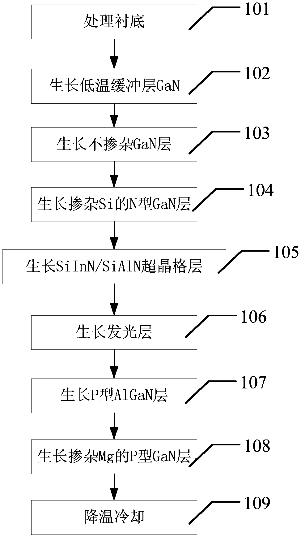
[0051] A kind of epitaxial growth method of current spreading layer, see figure 1 , including: processing the substrate, growing a low-temperature buffer layer GaN, growing an undoped GaN layer, growing a Si-doped N-type GaN layer, growing a light-emitting layer, growing a P-type AlGaN layer, and growing a Mg-doped P-type GaN layer , ...

Embodiment 2

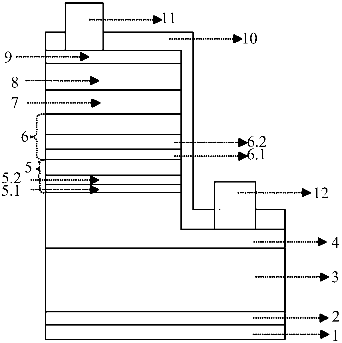
[0062] The application examples of the epitaxial growth method of the current spreading layer of the present invention are provided below, and its epitaxial structure can be found in figure 2 , growth method see figure 1 . Using MOCVD to grow high-brightness GaN-based LED epitaxial wafers. Using high-purity H 2 or high purity N 2 or high purity H 2 and high purity N 2 The mixed gas as the carrier gas, high-purity NH 3 As the N source, the metal-organic source trimethylgallium (TMGa) is used as the gallium source, trimethylindium (TMIn) is used as the indium source, and the N-type dopant is silane (SiH 4 ), trimethylaluminum (TMAl) as the aluminum source, and the P-type dopant as magnesium dicene (CP 2 Mg), the substrate is (0001) sapphire, and the reaction pressure is between 70mbar and 900mbar. The specific growth method is as follows:

[0063] Step 101, processing the substrate:

[0064] H at 1000°C-1100°C 2 Under the atmosphere, feed 100L / min-130L / min of H 2 , ...

Embodiment 3

[0089] A conventional LED epitaxial growth method is provided below as a comparative example of the present invention.

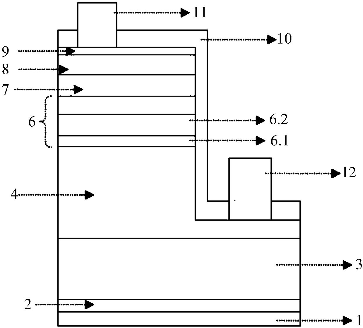
[0090] The growth method of conventional LED epitaxy is (see the epitaxial layer structure image 3 ):

[0091] 1. H at 1000°C-1100°C 2 Under the atmosphere, feed 100L / min-130L / min of H 2 , keep the reaction chamber pressure at 100mbar-300mbar, and process the sapphire substrate for 8min-10min.

[0092] 2. Lower the temperature to 500°C-600°C, keep the reaction chamber pressure at 300mbar-600mbar, and feed the flow rate at 10000sccm-20000sccm NH 3 , 50sccm-100sccm TMGa, 100L / min-130L / min H 2 , grow a low-temperature buffer layer GaN with a thickness of 20nm-40nm on a sapphire substrate.

[0093] 3. Raise the temperature to 1000°C-1200°C, keep the pressure in the reaction chamber at 300mbar-600mbar, and feed NH with a flow rate of 30000sccm-40000sccm 3 , 200sccm-400sccm TMGa, 100L / min-130L / min H 2 , Continuous growth of 2μm-4μm undoped GaN layer.

[0...


PUM


Abstract

The invention discloses an epitaxial growth method for a current expansion layer. The epitaxial growth method sequentially comprises the following steps of: processing a substrate, growing a low-temperature buffer layer GaN, growing a non-doped GaN layer, growing a Si-doped N type GaN layer, growing a SiInN / SiAlN super-lattice current expansion layer, growing a light emitting layer, growing a P type AlGaN layer, growing a Mg-doped P type GaN layer, and decreasing the temperature to cool. Conditions for producing the SiInN / SiAlN super-lattice current expansion layer are as follows: the pressure of a reaction chamber is kept at 300-400 mbar; the temperature is kept at 800-900 DEG C; and NH<3>, the flow of which is 30000-60000sccm, TMAl, the flow of which is 100-200sccm, TMIn, the flow of which is 1000-2000sccm, N<2>, the flow of which is 100-130L / min, and SiH<4>, the flow of which is 1-5sccm, are introduced.

Description

technical field [0001] The present application relates to the technical field of LED epitaxial design application, in particular, to an epitaxial growth method of a current spreading layer. Background technique [0002] At present, LED (Light Emitting Diode, light-emitting diode) is a kind of solid-state lighting. Its advantages such as small size, low power consumption, long service life, high brightness, environmental protection, and durability are recognized by consumers, and the scale of domestic production of LEDs is gradually expanding. ; The demand for LED brightness and luminous efficacy is increasing day by day in the market. How to grow better epitaxial wafers has been paid more and more attention. Because of the improvement of the quality of epitaxial layer crystals, the performance of LED devices can be improved, and the luminous efficiency, life, anti-aging ability, The antistatic ability and stability will increase with the improvement of the crystal quality of...

Claims


Application Information

Patent Timeline
Patent Type & Authority Patents(China)
IPC IPC(8): H01L33/14H01L33/04H01L33/00
CPCH01L33/0066H01L33/0075H01L33/04H01L33/14
Inventor 张宇
Owner XIANGNENG HUALEI OPTOELECTRONICS
Why Eureka
Try Eureka