Manufacturing method of flexible heat sink based on graphene large specific surface area
A technology with a large specific surface area and a manufacturing method, which is applied to semiconductor devices, electric solid-state devices, semiconductor/solid-state device components, etc., to achieve the effect of simple heat dissipation, efficient and reliable performance, and enhanced heat emission.
- Summary
- Abstract
- Description
- Claims
- Application Information
AI Technical Summary
Problems solved by technology
Method used
Image
Examples
Embodiment 1
[0033] A kind of manufacturing method based on graphene large specific surface area flexible radiator, comprises the following steps:
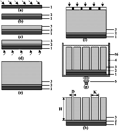
[0034] 1) Reference figure 1 , to prepare a high aspect ratio micro-hole array mold: refer to figure 1 (a), first use surface plasma to carry out surface activation treatment to smooth copper base 1; figure 1 (b), then the copper substrate 1 surface deposition layer thickness is the silver conductive film 2 of 300nm; figure 1 (c), 1(d) and 1(e), select SU-8 negative photoresist, and obtain a photoresist coating with a thickness of 500 μm through multiple coatings, pre-baking, re-leveling, and pre-baking ; refer to figure 1 (f), by exposing for 50 seconds each time and exposing 10 times, the ultraviolet exposure reaches the exposure dose; the post-baking of the photoresist is completed by stepping the temperature at intervals of 5°C and cooling down; refer to figure 1 (g), then use the special developing solution 4 in the developing tank 16...
Embodiment 2
[0042] A kind of manufacturing method based on graphene large specific surface area flexible radiator, comprises the following steps:
[0043] 1) Reference figure 1 , to prepare a high aspect ratio micro-hole array mold: refer to figure 1 (a), first use the mixed solution of sulfuric acid and hydrogen peroxide to carry out surface activation treatment to smooth aluminum substrate 1, the volume ratio of sulfuric acid and hydrogen peroxide is 2:1; Refer to figure 1 (b), then aluminum substrate 1 surface deposition thickness is the platinum conductive film 2 of 1000nm; figure 1 (c), 1(d) and 1(e), select SU-8 negative photoresist, and obtain a photoresist coating with a thickness of 50000 μm through multiple coatings, pre-baking, re-leveling, and pre-baking ; refer to figure 1 (f), by exposing for 1000 seconds each time, 10 times of sub-exposure, UV exposure reaches the exposure dose; adopt stepwise heating and cooling at intervals of 15°C to complete the post-baking of the ph...
Embodiment 3
[0051] A kind of manufacturing method based on graphene large specific surface area flexible radiator, comprises the following steps:
[0052] 1) Reference figure 1 , to prepare a high aspect ratio micro-hole array mold: refer to figure 1 (a), first use surface plasma to carry out surface activation treatment to smooth graphite plate substrate 1; figure 1 (b), then the graphite plate substrate 1 surface deposition layer thickness is the conductive film 2 of 700nm, and the conductive film 2 is an ITO film; figure 1 (c), 1(d) and 1(e), select SU-8 negative photoresist, and obtain a photoresist coating with a thickness of 25000 μm through multiple coatings, pre-baking, re-leveling, and pre-baking ; refer to figure 1 (f), by exposing for 1500 seconds each time and exposing 10 times, the ultraviolet exposure reaches the exposure dose; the post-baking of the photoresist is completed by stepping the temperature at intervals of 10°C and cooling down; refer to figure 1 (g), then us...
PUM
| Property | Measurement | Unit |
|---|---|---|
| thickness | aaaaa | aaaaa |
| thickness | aaaaa | aaaaa |
| diameter | aaaaa | aaaaa |
Abstract
Description
Claims
Application Information


