

Large-area heat sink structure for large power semiconductor device
A technology with a heat dissipation structure and a large area, which is used in semiconductor devices, semiconductor/solid-state device components, and electric solid-state devices to achieve the effects of reducing chip thermal resistance, low cost, and short heat flow paths.
- Summary
- Abstract
- Description
- Claims
- Application Information
AI Technical Summary
Problems solved by technology
Method used
Image

Examples
Embodiment 1
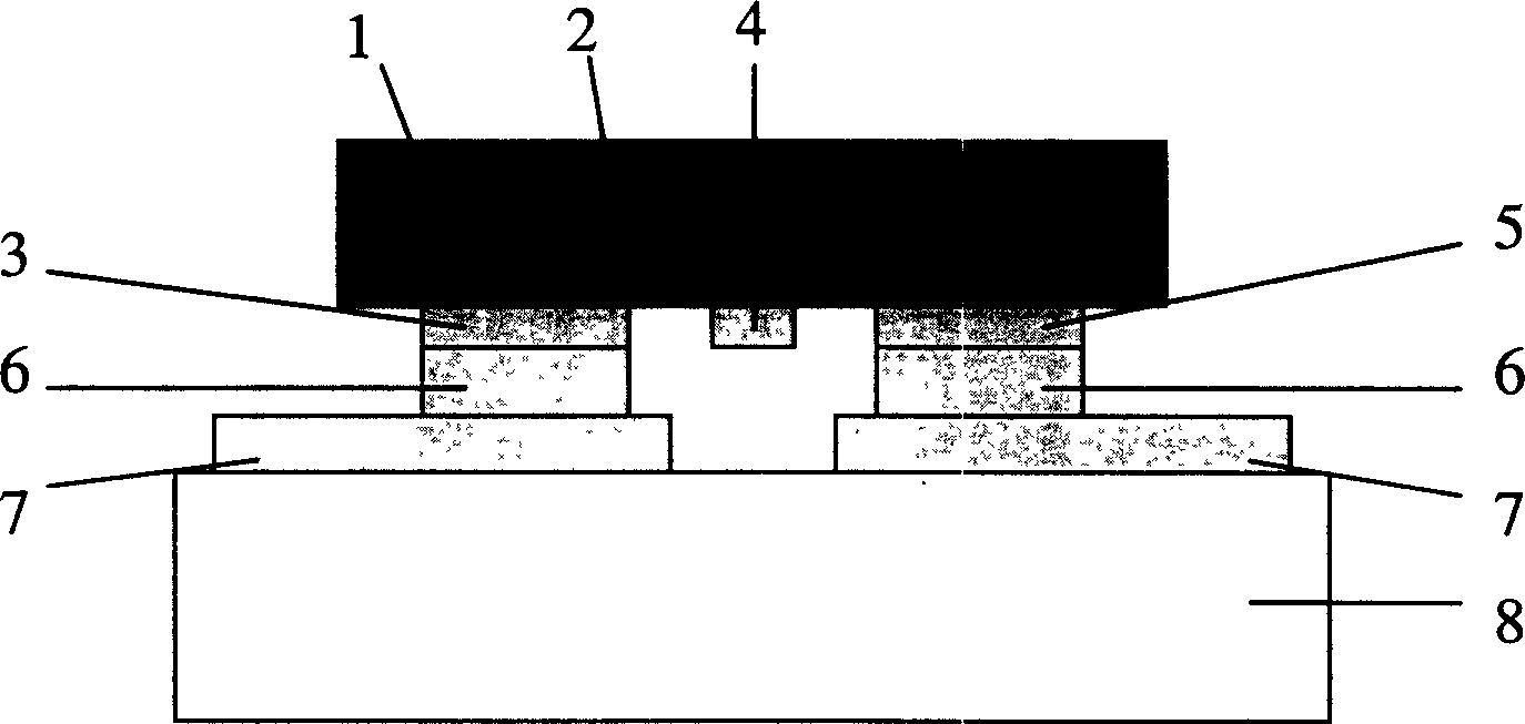
[0038] The sapphire substrate AlGaN / GaN HEMT large-area flip chip structure disclosed by the present invention is as follows: figure 2 As shown: 1 is the sapphire substrate, 2 is the epitaxial layer, on which the AlGaN / GaN HEMT device is fabricated, 3 is the source pad of the device, 4 is the gate electrode, 5 is the drain pad, 9 is the copper bump 10 is the lead-tin solder joint, 11 and 12 are gold pads and copper pads on the Si-based heat sink 13, 7 is the heat sink electrode, and 14 is the silicon nitride heat-conducting insulating film. During the chip manufacturing process, the HEMT device is manufactured by conventional technology; then the silicon nitride thermal insulating film is deposited on the front of the chip by plasma enhanced chemical vapor deposition (PECVD); layer and flip-chip soldering bumps; at the same time, a similar process is used to deposit silicon nitride film on the Si-based heat sink, open electrode lead-out holes, and make an adhesion layer and f...
Embodiment 2
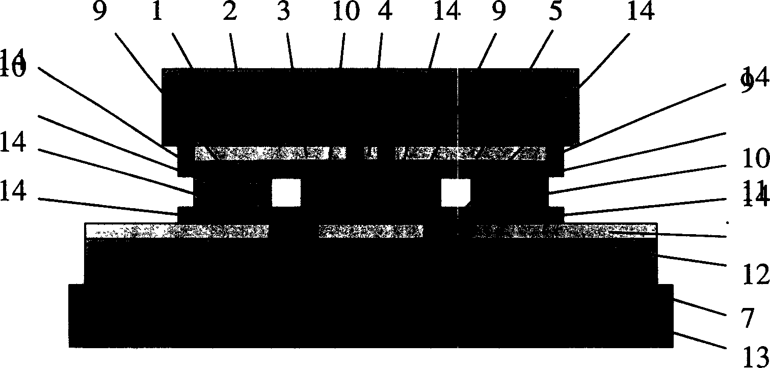
[0042] The sapphire substrate AlGaN / GaN HEMT large-area flip chip structure disclosed by the present invention is as follows: Figure 6 As shown: 1 is the sapphire substrate, 2 is the epitaxial layer, on which the AlGaN / GaN HEMT device is fabricated, 3, 4, and 5 are the source pad, gate electrode, and drain pad of the device, and 9 is copper Bump, 14 is a silicon nitride heat conduction insulating film, 81 is a heat sink under the Si base, and 82 is a heat sink on the Si base. The manufacturing process of the device is basically the same as that of Embodiment 1, except that the substrate is thinned, and a heat sink is installed on one side of the substrate to form a double-sided heat dissipation structure, which further reduces the thermal resistance of the chip. Experiments have proved that the output power density of the flip-chip AlGaN / GaN HEMT chip with double-sided heat dissipation structure produced in this example can be increased by more than 60% under the same conditi...
PUM
| Property | Measurement | Unit |
|---|---|---|
| Thickness | aaaaa | aaaaa |
| Thickness | aaaaa | aaaaa |
Abstract
Description
Claims
Application Information