A kind of encapsulation process of LED display module
A technology of LED display and packaging technology, which is applied in the direction of identification devices, instruments, semiconductor devices, etc., can solve the problems of insufficient display effect and low resolution, and achieve better and more delicate display effect, improved resolution, and improved reliability. Effect
- Summary
- Abstract
- Description
- Claims
- Application Information
AI Technical Summary
Problems solved by technology
Method used
Image
Examples
Embodiment Construction
[0019] In conjunction with the accompanying drawings, the specific implementation manners of the present invention will be further described in detail, so as to make the technical solution of the present invention easier to understand and grasp.
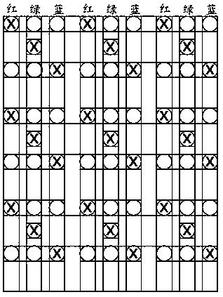
[0020] A packaging process for an LED display module, comprising the following steps:
[0021] 1) The red, blue and green display chips are sealed on the surface of the colloid according to the law;
[0022] 2) Plating the first layer of conductive film on the back of the red, blue and green display chips, and carving off the excess film to form the required conductive lines, so that the chips are connected in series;
[0023] 3) Cover a layer of protective layer on the first layer of conductive film, and carve off the protective layer of each chip pad (BOND PAD) to expose the pad;
[0024] 4) Plating a second layer of conductive film on the protective layer, and carving off the excess film to form the required conductive line, and ...
PUM
 Abstract
Description
Claims
Application Information
