A Packed Layout Method for Adders

A layout method and adder technology, which is applied in the fields of instruments, computing, electrical digital data processing, etc., can solve problems such as not being able to find the optimal solution, and achieve the effect of reducing wiring resources

Active Publication Date: 2019-12-13
CAPITAL MICROELECTRONICS
View PDF4 Cites 0 Cited by
  • Summary
  • Abstract
  • Description
  • Claims
  • Application Information

AI Technical Summary

Problems solved by technology

However, due to the limitations of the algorithm, it is often impossible to find all the optimal solutions.
[0004] At present, the industry has not proposed a good guarantee to solve the problem of extracting a usage mode to match the user's design mode based on the inherent fast line resources of the chip.

Method used


Image

  • A Packed Layout Method for Adders
  • A Packed Layout Method for Adders
  • A Packed Layout Method for Adders

Examples


Embodiment Construction

[0019] In order to make the purpose, technical solutions and advantages of the embodiments of the present invention clearer, the technical solutions in the embodiments of the present invention will be clearly and completely described below in conjunction with the drawings in the embodiments of the present invention. Obviously, the described embodiments It is a part of embodiments of the present invention, but not all embodiments.

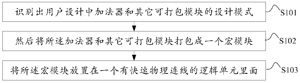
[0020] An embodiment of the present invention provides a packaging and layout method of an adder, which can match a user's design mode through a usage mode according to the inherent fast line resources of the chip. After matching, the wiring resources used by the adder and other modules are reduced, and the delay is also reduced while the wiring resource usage is reduced.

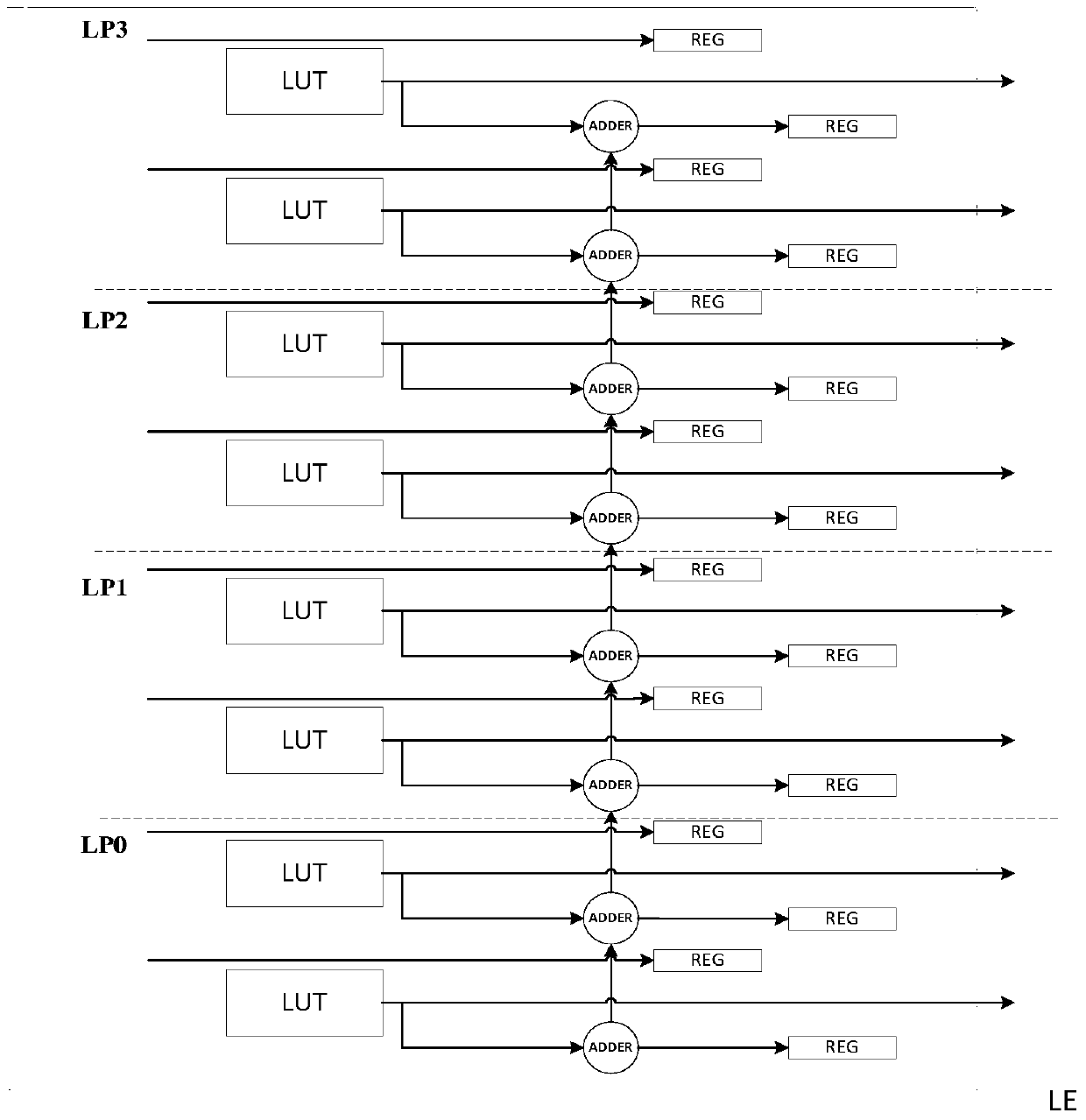
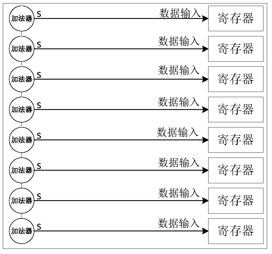
[0021] figure 1 It is a schematic flowchart of a packing and layout method for an adder provided by an embodiment of the present invention. Such as figure 1 As shown, a packin...


PUM


Abstract

The invention relates to a method for packing and deploying adders. The method includes the steps of: identifying the design mode of the adders and other packageable modules in a design of a user; then packing the adders and other packageable modules into one macro block; and disposing the macro block in a logic unit with a fast physical connection line. According to the invention, the design mode of the user can be matched through a usage mode according to the inherent fast line resource of a chip; and after the design mode of the user is matched, the line routing resources used by the adders and other modules are reduced, thereby reducing usage of line routing resources and also reducing the time delay.

Description

technical field [0001] The invention relates to the technical field of integrated circuits, in particular to a packing and layout method of an adder. Background technique [0002] Currently, in Field Programmable Gate Array (Field Programmable Gate Array, FPGA) applications, integrated circuits are required to have a programmable or configurable interconnection network, and logic gates are connected to each other through the configurable interconnection network. FPGAs, functioning as stand-alone chips or as a core part of a system, have been widely used in a large number of microelectronic devices. The definition of FPGA logic gate in a broad sense not only refers to simple NAND gates, but also refers to logic units of combinational logic and sequential logic with configurable functions or logic blocks composed of multiple logic units interconnected. [0003] There is a short-distance physical connection on the chip hardware, and the delay is short, which belongs to the lev...

Claims


Application Information

Patent Timeline
Patent Type & Authority Patents(China)
IPC IPC(8): G06F17/50
Inventor 蒋中华黄攀
Owner CAPITAL MICROELECTRONICS
Why Eureka
Try Eureka