

Camera shooting optical lens
An optical lens and lens technology, applied in the field of optical lenses, can solve problems such as inability to meet, and achieve the effect of improving imaging quality and good sensitivity performance
- Summary
- Abstract
- Description
- Claims
- Application Information
AI Technical Summary
Problems solved by technology
Method used
Image

Examples
Embodiment Construction
[0016] In order to make the object, technical solution and advantages of the present invention clearer, various embodiments of the present invention will be described in detail below in conjunction with the accompanying drawings. However, those of ordinary skill in the art can understand that in each implementation manner of the present invention, many technical details are proposed in order to enable readers to better understand the present invention. However, even without these technical details and various changes and modifications based on the following implementation modes, the technical solution claimed in the present invention can also be realized.
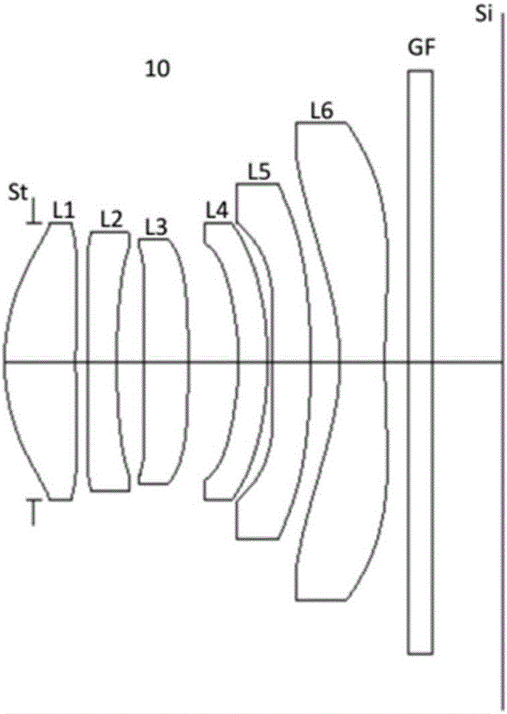
[0017] With reference to the accompanying drawings, the present invention provides an imaging optical lens. figure 1 Shown is the imaging optical lens 10 of the first embodiment of the present invention, and the imaging optical lens 10 includes six lenses. Specifically, the photographing optical lens 10 includes in sequenc...
PUM
| Property | Measurement | Unit |
|---|---|---|
| Optical total length | aaaaa | aaaaa |
Abstract
Description
Claims
Application Information