Antenna system and communication terminal having antenna system
An antenna system and communication terminal technology, which is applied to antennas, antenna parts, antenna grounding devices, etc., can solve the problems of communication terminal antenna performance limitations, strong metal back cover, and unsatisfactory antenna performance, etc., to improve GPS positioning performance, reduce the sense of fragmentation, and reduce the effect of loss
- Summary
- Abstract
- Description
- Claims
- Application Information
AI Technical Summary
Problems solved by technology
Method used
Image


Examples
Embodiment Construction
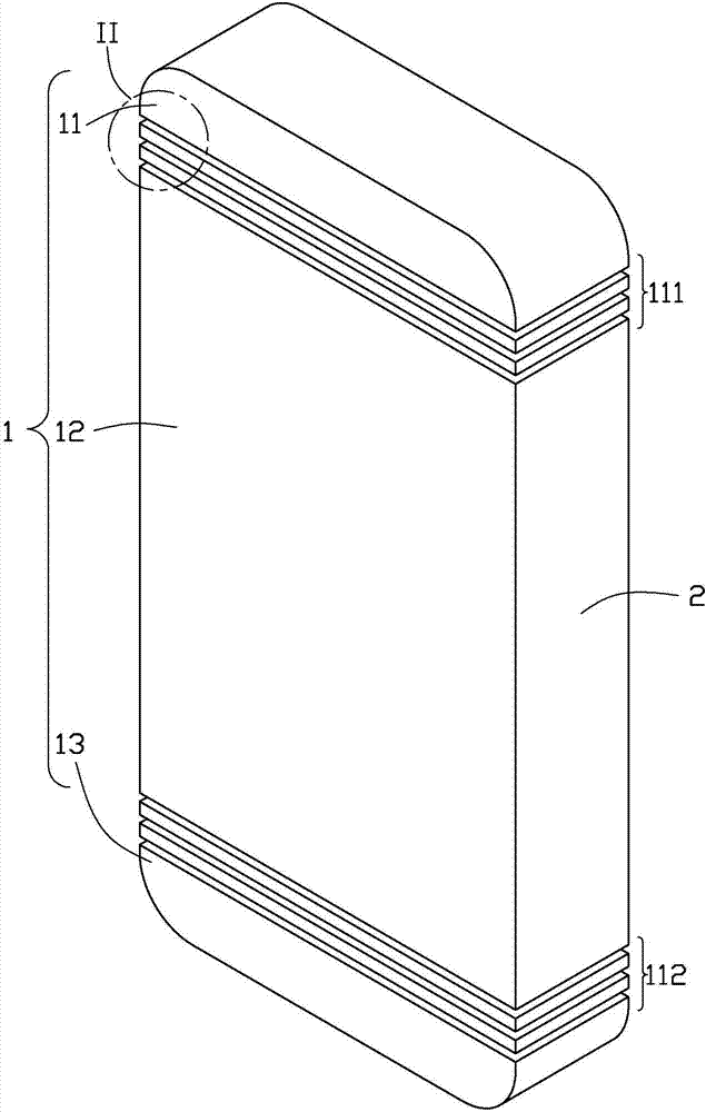
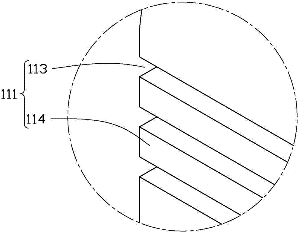
[0027] In order to make the purpose, technical solution and advantages of the present invention clearer, the present invention will be clearly and completely described below in conjunction with the accompanying drawings and specific embodiments. Apparently, the described embodiments are only some of the embodiments of the present invention, but not all of them. Based on the embodiments of the present invention, all other embodiments obtained by persons of ordinary skill in the art without making creative efforts belong to the protection scope of the present invention.
[0028] It should be noted that when a component is said to be "fixed" to another component, it can be directly on the other component or there can also be an intervening component. When a component is said to be "connected" to another component, it may be directly connected to the other component or there may be intervening components at the same time. When a component is said to be "set on" another component,...
PUM
 Abstract
Description
Claims
Application Information