

Strain test equipment of nanometer resolution and method thereof
A strain measurement and resolution technology, applied in measurement devices, instruments, and the use of wave/particle radiation, etc., can solve the problems of inaccurate and fine testing, poor applicability, and inability to perform real-time dynamic testing, achieving convenient testing process and comprehensive functions. Effect
Active Publication Date: 2017-08-25
常州满旺半导体科技有限公司
View PDF6 Cites 0 Cited by
- Summary
- Abstract
- Description
- Claims
- Application Information
AI Technical Summary
Problems solved by technology
XRD or Raman spectroscopy is used to measure lattice constants to estimate strain. Due to the difficulty of focusing light waves and the fact that light spots are generally on the order of microns or submicrons, it is difficult to achieve nanometer-level resolution testing; and there are many test conditions, such as Raman spectroscopy. Fluorescence must be avoided, and a microscope must be used to focus t
Method used
View moreImage
Smart ImageViewing Examples

Examples
 PUM
| Property | Measurement | Unit |
|---|---|---|
| Thickness | aaaaa | aaaaa |
| Thickness | aaaaa | aaaaa |
| Thickness | aaaaa | aaaaa |
Abstract
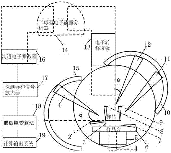
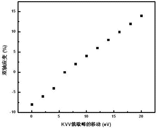
The invention discloses strain test equipment of a nanometer resolution and a method thereof. The equipment comprises a test chamber, a sample bench, a temperature magnetic field control apparatus below the sample bench, a mobile motor, a sample to be measured placed on the sample bench, a first probe, a second probe, a third probe, a fourth probe, an electronic gun, a first rotation track, an X ray gun, an ion gun and a second rotation track, wherein the first probe and the second probe are arranged above a sample; the third probe and the fourth probe are arranged on a sample side wall or a cross section; the electronic gun possesses multiple focusing electron beams; the first rotation track controls rotation of the electronic gun; and the second rotation track controls the rotation of the ion gun. An auger electron spectrums collected by the test chamber are transmitted to a detector and a signal amplifier successively through an electron transfer lens, a semi-spherical electronic energy analyzer and a channel electron multiplier. The detector and signal amplifier output a dynamic strain value epsilon of the sample in real time through an auger strain algorithm module and a calculating output system.
Description
technical field [0001] The invention relates to a strain testing device and method, in particular to a high-precision strain testing device and method for testing semiconductor materials. Background technique [0002] The test of strain in solid or thin film materials generally adopts the following three methods: 1) use the lattice constant change obtained by XRD measurement to estimate the size of the strain; 2) calculate the strain according to the frequency shift of the Raman spectrum; 3) use HRTEM measures changes in atomic lattice spacing to calculate strain. XRD or Raman spectroscopy is used to measure lattice constants to estimate strain. Due to the difficulty of focusing light waves and the fact that light spots are generally on the order of microns or submicrons, it is difficult to achieve nanometer-level resolution testing; and there are many test conditions, such as Raman spectroscopy. Fluorescence must be avoided, and a microscope must be used to focus the light...
Claims
Login to View More Application Information
Patent Timeline
 IPC IPC(8): G01B15/06
CPCG01B15/06
Inventor郑锦坚郑清团王星河康俊勇
Owner常州满旺半导体科技有限公司