Array substrate, liquid crystal display device and driving method

A technology for liquid crystal display devices and array substrates, applied in static indicators, instruments, nonlinear optics, etc., can solve the problem of uneven display of image quality, reduce signal coupling, solve uneven display of images, and improve display image quality Effect

Active Publication Date: 2020-08-04
KUSN INFOVISION OPTOELECTRONICS
View PDF4 Cites 0 Cited by
  • Summary
  • Abstract
  • Description
  • Claims
  • Application Information

AI Technical Summary

Problems solved by technology

[0008] The purpose of the present invention is to provide an array substrate, a liquid crystal display device and a driving method, which can realize switching between wide and narrow viewing angles in different occasions, and improve the problem of uneven display quality

Method used


Image

  • Array substrate, liquid crystal display device and driving method
  • Array substrate, liquid crystal display device and driving method
  • Array substrate, liquid crystal display device and driving method

Examples


no. 1 example

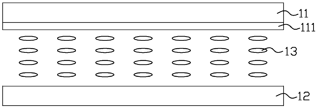
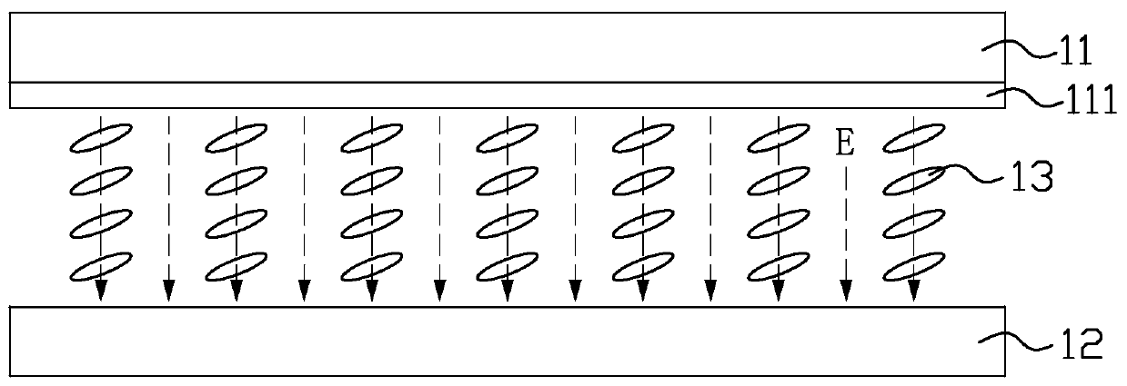
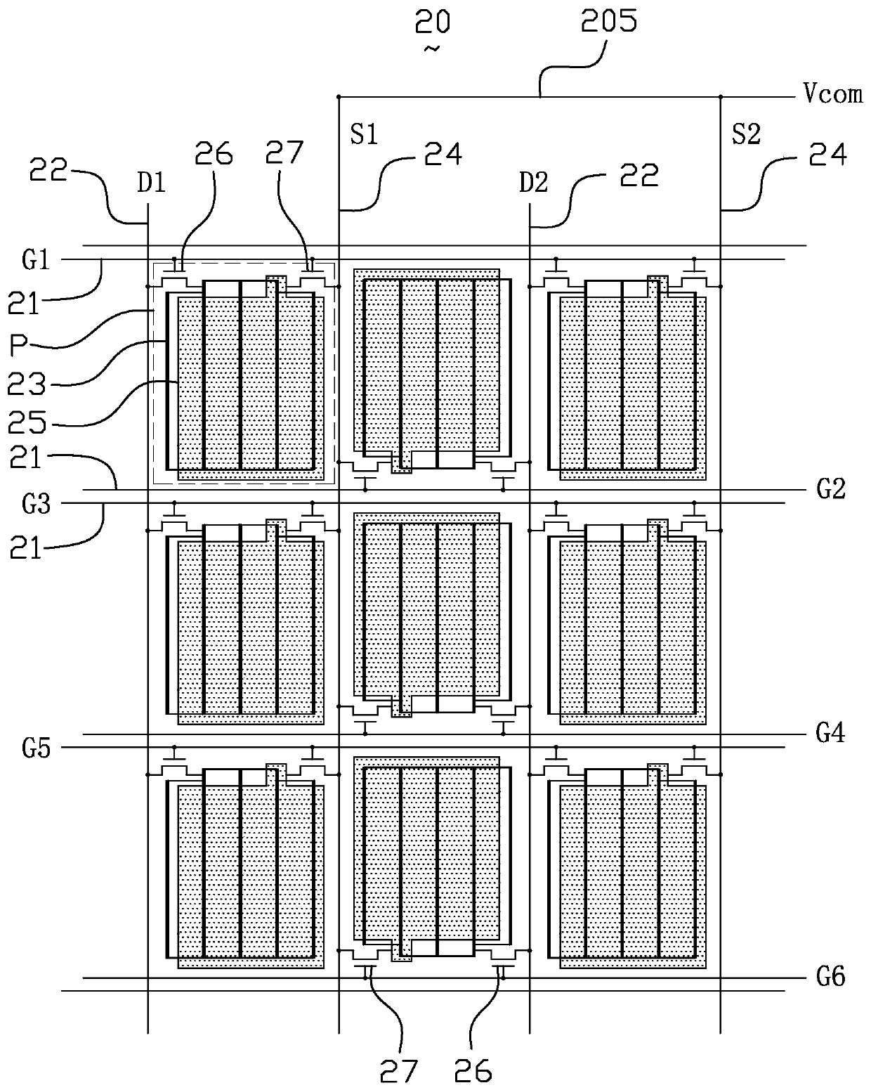
[0042] Please refer Figure 3 to Figure 5 The first embodiment of the present invention provides an array substrate 20. The array substrate 20 is provided with a plurality of scan lines 21 (G1, G2,..., Gn) and a plurality of data lines 22 (D1, D2,..., Dn). , A plurality of pixel electrodes 23, a plurality of common lines 24 (S1, S2, ..., Sn), a plurality of common electrode blocks 25, a plurality of first thin film transistors 26, and a plurality of second thin film transistors 27.

[0043] The plurality of common lines 24 and the plurality of data lines 22 extend in the same direction and are alternately arranged with each other. For example, the common lines 24 and the data lines 22 both extend in the vertical direction, and the plurality of common lines 24 and the plurality of data lines Alternate arrangement, that is, a common line 24 is provided between two adjacent data lines 22, and a data line 22 is provided between two adjacent common lines 24. Specifically, the plurali...

no. 2 example

[0056] Please refer Image 6 The second embodiment of the present invention provides an array substrate 20. The main difference between this embodiment and the above-mentioned first embodiment is that in the array substrate 20 of this embodiment, the first thin film transistor 26 and the The second thin film transistors 27 are arranged diagonally and are respectively connected to different scan lines 21 located on the upper and lower sides of the pixel unit P. For example, taking a pixel unit P in the first row as an example, the first thin film transistor 26 in the pixel unit P is connected to the scan line G1 located on the upper side of the pixel unit P, and the second thin film transistor 27 in the pixel unit P Connected to the scan line G2 located on the lower side of the pixel unit P; or, the first thin film transistor 26 in the pixel unit P is connected to the scan line G2 located on the lower side of the pixel unit P, and the first thin film transistor 26 in the pixel un...

no. 3 example

[0060] Please refer Figure 7 The third embodiment of the present invention provides an array substrate 20. The main difference between this embodiment and the above-mentioned first embodiment is that in the array substrate 20 of this embodiment, each pixel unit P is provided with a first thin film transistor. 26 and a pixel electrode 23. The pixel electrode 23 in each pixel unit P is electrically connected to the data line 22 adjacent to the first thin film transistor 26 through the first thin film transistor 26. In the horizontal direction, a second thin film transistor 27 and a common electrode block 25 are provided in every two adjacent pixel units P, that is, each common electrode block 25 corresponds to two pixel units P, and every two adjacent pixel units P The common electrode block 25 in the pixel unit P is electrically connected to the common line 24 adjacent to the second thin film transistor 27 through the second thin film transistor 27.

[0061] In this embodiment, t...


PUM


Abstract

The invention provides an array substrate, a liquid crystal display device and a driving method. The array substrate is provided with a plurality of scanning lines, a plurality of data lines, a plurality of pixel electrodes and a plurality of first thin film transistors and further provided with a plurality of public lines, a plurality of public electrode blocks and a plurality of second thin film transistors. The scanning lines, the data lines and the public lines are insulated and crossed to define and form a plurality of pixel units. Two lines of pixel units are arranged between every two adjacent data lines, one public line is arranged between the two lines of pixel units, and two scanning lines are arranged between every two adjacent lines of pixel units. Each pixel unit is internally provided with one first thin film transistor, one pixel electrode, one second thin film transistor and one public electrode block. The pixel electrodes are connected with the data lines through the first thin film transistors. The public electrode blocks are connected with the public lines through the second thin film transistors. Wide vision and narrow vision can be switched on different occasions, and the problem that image quality display is not uniform is solved.

Description

Technical field [0001] The present invention relates to the technical field of liquid crystal display, in particular to an array substrate, a liquid crystal display device and a driving method. Background technique [0002] Liquid crystal display (LCD) has the advantages of good image quality, small size, light weight, low driving voltage, low power consumption, no radiation, and relatively low manufacturing cost, and it is dominant in the flat panel display field. [0003] With the continuous advancement of liquid crystal display technology, the viewing angle of the display has been widened from about 120° to more than 160°. While enjoying the visual experience brought by the large viewing angle, people also hope to effectively protect trade secrets and personal privacy. Avoid business losses or embarrassment caused by leakage of screen information. Therefore, in addition to the wide viewing angle, the display device needs to be switchable to a narrow viewing angle. [0004] The c...

Claims


Application Information

Patent Timeline
Patent Type & Authority Patents(China)
IPC IPC(8): G02F1/1362G02F1/1368G09G3/36
CPCG02F1/136286G02F1/1368G09G3/36
Inventor 钟德镇刘仕彬乔艳冰
Owner KUSN INFOVISION OPTOELECTRONICS
Why Eureka
Try Eureka