Array substrate, liquid crystal display device, and driving method
A technology of liquid crystal display devices and array substrates, which is applied in static indicators, instruments, nonlinear optics, etc., can solve the problem of uneven display of image quality, achieve the effects of reducing signal coupling, increasing charging time, and improving display image quality
- Summary
- Abstract
- Description
- Claims
- Application Information
AI Technical Summary
Problems solved by technology
Method used
Image
Examples
no. 1 example
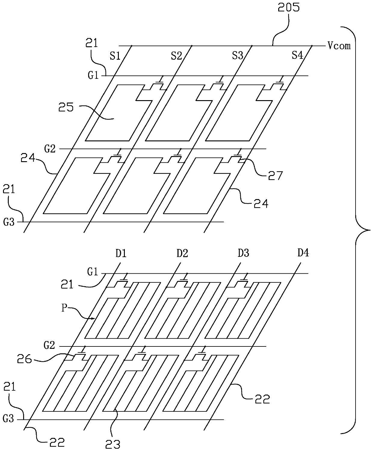
[0044] Please refer to Figure 3 to Figure 5 , the first embodiment of the present invention provides an array substrate 20, the array substrate 20 is provided with a plurality of scanning lines 21, a plurality of data lines 22, a plurality of pixel electrodes 23, a plurality of common lines 24, a plurality of common electrode blocks 25 . A plurality of first thin film transistors 26 and a plurality of second thin film transistors 27 .
[0045] The plurality of scan lines 21 and the plurality of data lines 22 are insulated and intersect to define a plurality of pixel units P arranged in an array, and each pixel unit P is defined by two scan lines 21 and two data lines 22 .
[0046] The plurality of common lines 24 and the plurality of data lines 22 extend in the same direction and are arranged to overlap up and down. For example, the common lines 24 and the data lines 22 both extend along the vertical direction. The intervals can be completely overlapped or mostly overlapped,...
no. 2 example
[0059] Please refer to Figure 6 to Figure 7 The second embodiment of the present invention provides an array substrate 20. The main difference between this embodiment and the above-mentioned first embodiment is that in the array substrate 20 of this embodiment, the plurality of common lines 24 are located at the plurality of data lines 22 directly below the Image 6 In order to facilitate drawing, the upper data line 22 is drawn narrower than the lower common line 24, but this should not be regarded as a limitation of the present invention. Specifically, each common line 24 and the corresponding data line 22 may completely overlap, or mostly overlap, that is, there may be a certain small misalignment between the two.
[0060] The array substrate 20 is also provided with a first conduction hole 201 that connects the pixel electrode 23 to the drain of the first thin film transistor 26, and a second conduction hole 201 that connects the common electrode block 25 to the drain of...
no. 3 example
[0064] Please refer to Figure 8 The third embodiment of the present invention provides an array substrate 20. The main difference between this embodiment and the above-mentioned first embodiment is that in the array substrate 20 of this embodiment, the first thin film transistor 26 and the first thin film transistor 26 in each pixel unit P The second thin film transistors 27 are arranged diagonally and are respectively connected to different scanning lines 21 located on the upper and lower sides of the pixel unit P. For example, taking a pixel unit P in the first row as an example, the first thin film transistor 26 in the pixel unit P is connected to the scanning line G1 on the upper side of the pixel unit P, and the second thin film transistor 27 in the pixel unit P is connected to the scanning line G2 on the lower side of the pixel unit P; or, the first thin film transistor 26 in the pixel unit P is connected to the scanning line G2 on the lower side of the pixel unit P, an...
PUM
 Abstract
Description
Claims
Application Information


