Array substrate and pixel unit of display panel

一种显示面板、阵列基板的技术,应用在电气元件、静态指示器、光学等方向,能够解决源极驱动芯片成本增加、像素充电时间不足、开口率降低等问题

Active Publication Date: 2012-10-24
AU OPTRONICS CORP
View PDF5 Cites 19 Cited by
  • Summary
  • Abstract
  • Description
  • Claims
  • Application Information

AI Technical Summary

Problems solved by technology

With the increase in the number of gate lines and data lines and the frame update rate, LCDs will face problems such as increased cost of source driver chips, reduced aperture ratio, and insufficient pixel charging time.

Method used


Image

  • Array substrate and pixel unit of display panel
  • Array substrate and pixel unit of display panel
  • Array substrate and pixel unit of display panel

Examples


Embodiment Construction

[0026] In order for those skilled in the art to have a better understanding of the present invention, preferred embodiments of the present invention are enumerated below, together with the accompanying drawings, to describe in detail the composition and desired effects of the present invention.

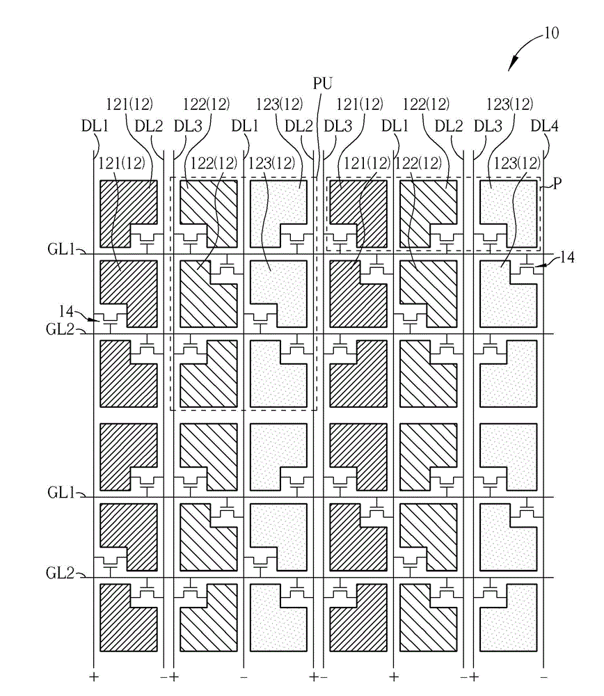
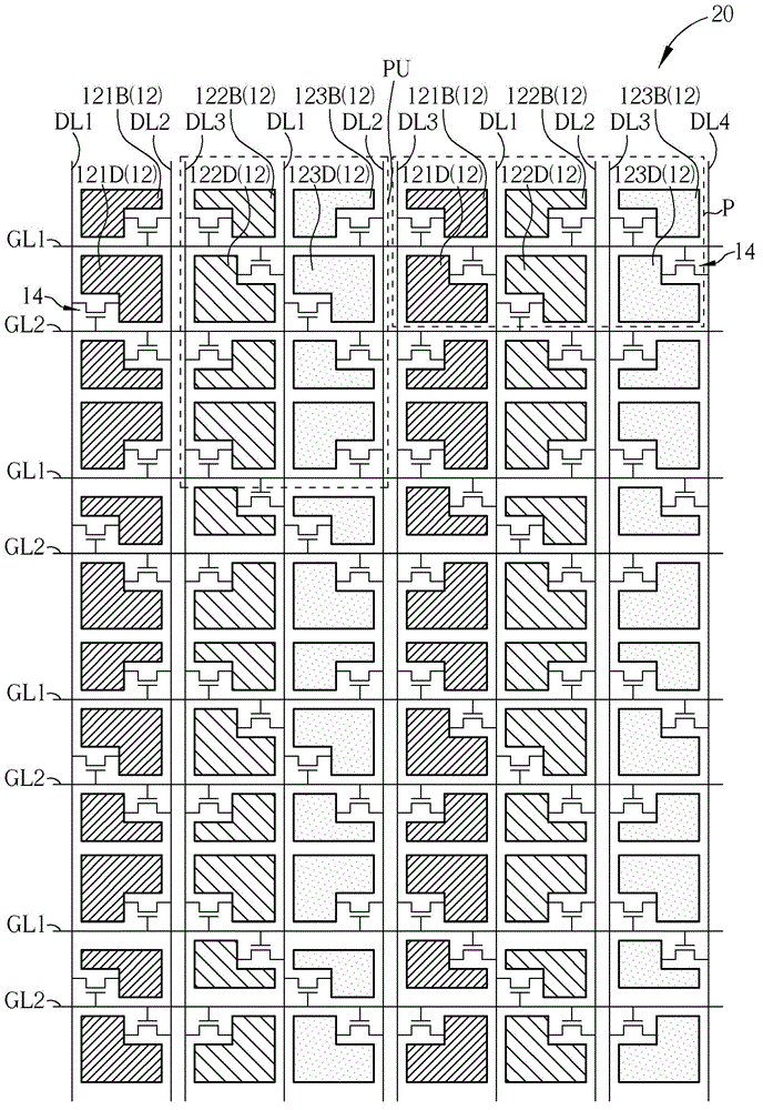
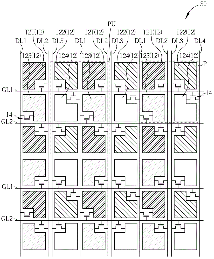
[0027] Please refer to figure 1 . figure 1 is a schematic diagram of the array substrate of the display panel according to the first preferred embodiment of the present invention. Such as figure 1 As shown, the array substrate 10 of the display panel of this embodiment includes a plurality of sub-pixels 12, a plurality of active switching elements 14, a plurality of first gate lines GL1, a plurality of second gate lines GL2, and a plurality of data lines ( It includes a plurality of first data lines DL1, a plurality of second data lines DL2, a plurality of third data lines DL3 and a fourth data line DL4). The sub-pixels 12 are arranged into a pixel array of N columns*M rows, wherei...


PUM


Abstract

An array substrate and a pixel unit of a display panel are provided. The array substrate comprises multiple sub pixels which are arranged in a pixel array having N lines and M rows. In the pixel array, only one data line is arranged between a part of the sub pixels in two adjacent rows, and two data lines are arranged between a part of the sub pixels in two adjacent rows.

Description

technical field [0001] The present invention relates to an array substrate and a pixel unit of a display panel, in particular to an array substrate and a pixel unit of a display panel with a long charging time and low color shift and a high frame rate. . Background technique [0002] Because flat panel displays, such as liquid crystal displays, have the characteristics of thinness, lightness and small size, they have replaced cathode ray tube (CRT) displays and become the mainstream products of displays. However, taking liquid crystal display as an example, it is prone to color washout problem. The conventional method to solve the color washout problem is to double the number of data lines of the liquid crystal display panel. However, this method will make the source The cost of the electrode driver chip increases, the aperture ratio decreases, and the pixel charging time is insufficient. In addition, in order to pursue better display quality, the requirements for the reso...

Claims


Application Information

Patent Timeline
Patent Type & Authority Applications(China)
IPC IPC(8): G02F1/1362G02F1/133
CPCH01L33/08G02F1/136286G02F1/1362G02F1/1368G09G3/36G02F1/133G09G3/3607G09G3/3614G09G3/3659G09G3/3685G09G2300/0426G09G2300/0443G09G2300/0465G09G2340/0435
Inventor 江佳伦黄郁升蔡孟汝陈彦樵陈一清
Owner AU OPTRONICS CORP
Why Eureka
Try Eureka