Array substrate, liquid crystal display device and driving method
An array substrate and the technology of the same direction, applied in the field of liquid crystal display, can solve the problem of uneven display quality, achieve the effect of reducing signal coupling, preventing light leakage, and improving display quality
- Summary
- Abstract
- Description
- Claims
- Application Information
AI Technical Summary
Problems solved by technology
Method used
Image
Examples
no. 1 example
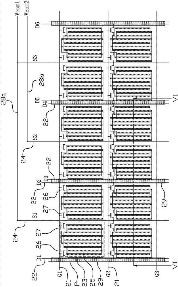
[0038] Please refer to Figure 3 to Figure 6 The first embodiment of the present invention provides a liquid crystal display device, which includes an array substrate 20, a color filter substrate 30 disposed opposite to the array substrate 20, and a liquid crystal layer 40 located between the array substrate 20 and the color filter substrate 30 .
[0039] The array substrate 20 is provided with a plurality of scanning lines 21, a plurality of data lines 22, a plurality of common lines 24, a plurality of pixel electrodes 23, a plurality of common electrodes 25, a plurality of first thin film transistors 26, and a plurality of second thin film transistors. 27 and a plurality of conductive strips 29.
[0040] The plurality of common lines 24 and the plurality of data lines 22 extend in the same direction, for example, the plurality of common lines 24 and the plurality of data lines 22 extend along the vertical direction, and the plurality of scanning lines 21 extend along the ho...
no. 2 example
[0065] Please refer to Figure 10 The difference between the liquid crystal display device provided by the second embodiment of the present invention and the above-mentioned first embodiment is that, in this embodiment, the pixel units P at the odd-numbered positions and the pixel units P at the even-numbered positions in each row are separately connected to the On the different scanning lines 21 on the upper and lower sides of the row of pixel units P, wherein the pixel units P located in odd positions in each row are connected to the scanning lines 21 located on the upper side of the row of pixel units P, and the pixel units P located in even positions in each row The pixel units P are connected to different scan lines 21 located on the lower side of the row of pixel units P.
[0066] For other structures and working principles of this embodiment, reference may be made to the above-mentioned first embodiment, which will not be repeated here.
no. 3 example
[0068] Please refer to Figure 11 The difference between the liquid crystal display device provided by the third embodiment of the present invention and the above-mentioned first embodiment is that, in this embodiment, a common electrode is provided in every two pixel units P between two adjacent groups of data lines 22 25 (that is, each common electrode 25 covers two pixel units P at the same time), and each common electrode 25 is connected to the scanning line 21 and the common line 24 adjacent to the second thin film transistor 27 through two second thin film transistors 27 . Specifically, in this embodiment, each common electrode 25 is located in two adjacent pixel units P between two groups of data lines 22 in the direction of the scanning line 21 . In one embodiment, each common electrode 25 may also be connected to the scan line 21 and the common line 24 adjacent to the second thin film transistor 27 through a second thin film transistor 27 .
[0069] For other structu...
PUM
 Abstract
Description
Claims
Application Information


