
Manufacturing method of bottom gate type tft substrate

A manufacturing method and substrate technology, which can be applied to semiconductor devices, electrical components, circuits, etc., can solve the problems of over-etching of source and drain, affecting the connection of source and drain contact resistance lines, etc.

Active Publication Date: 2019-12-24
TCL CHINA STAR OPTOELECTRONICS TECH CO LTD
View PDF5 Cites 0 Cited by
  • Summary
  • Abstract
  • Description
  • Claims
  • Application Information

AI Technical Summary

Problems solved by technology

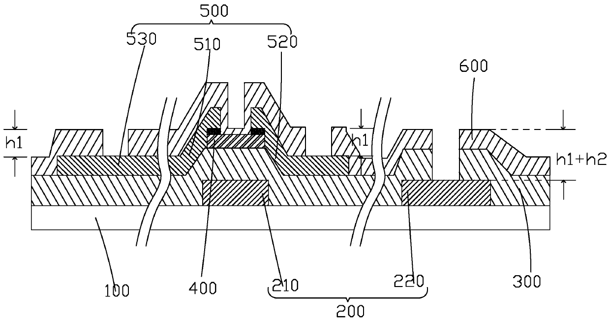
[0004] In addition, after the passivation layer 600 is formed, it is necessary to etch the source-drain metal layer 500 and the electrical insulation layer above the gate metal layer 200 to form through holes at one time, and then plate a light-transmitting conductive film to realize the gate. The electrode connection terminal 220, the source-drain connection terminal 530 are connected to the peripheral circuit, and the connection between the drain electrode 520 and the pixel electrode, etc., that is, it is necessary to etch and form a through hole on the passivation layer 600 above the source-drain metal layer 500. The gate insulating layer 300 above the gate metal layer 200 and the passivation layer 600 are etched to form a via hole, but in the etching process, forming a via hole above the source-drain metal layer 500 needs to etch the thickness of the electrical insulating layer to be the passivation layer. The thickness h1 of the layer 600, and the thickness h1+h2 of the passivation layer 600 plus the thickness h2 of the gate insulating layer 300 needs to be etched to form a via hole above the gate metal layer 200, and in order to ensure that the thickness above the gate metal layer 200 When the gate insulating layer 300 is etched through, it is often necessary to overcut by more than 30% on the basis of the thickness (h1+h2) of the electrical insulating layer above the gate metal layer 200. Therefore, during the etching process, the area above the source-drain metal layer 500 The electrical insulating layer will be scratched through first, causing the source and drain to be severely overcut, which will affect the source and drain contact resistance and line connection

Method used


Image

  • Manufacturing method of bottom gate type tft substrate
  • Manufacturing method of bottom gate type tft substrate
  • Manufacturing method of bottom gate type tft substrate

Examples


Embodiment Construction

[0036]In order to further illustrate the technical means adopted by the present invention and its effects, the following describes in detail in conjunction with preferred embodiments of the present invention and accompanying drawings.

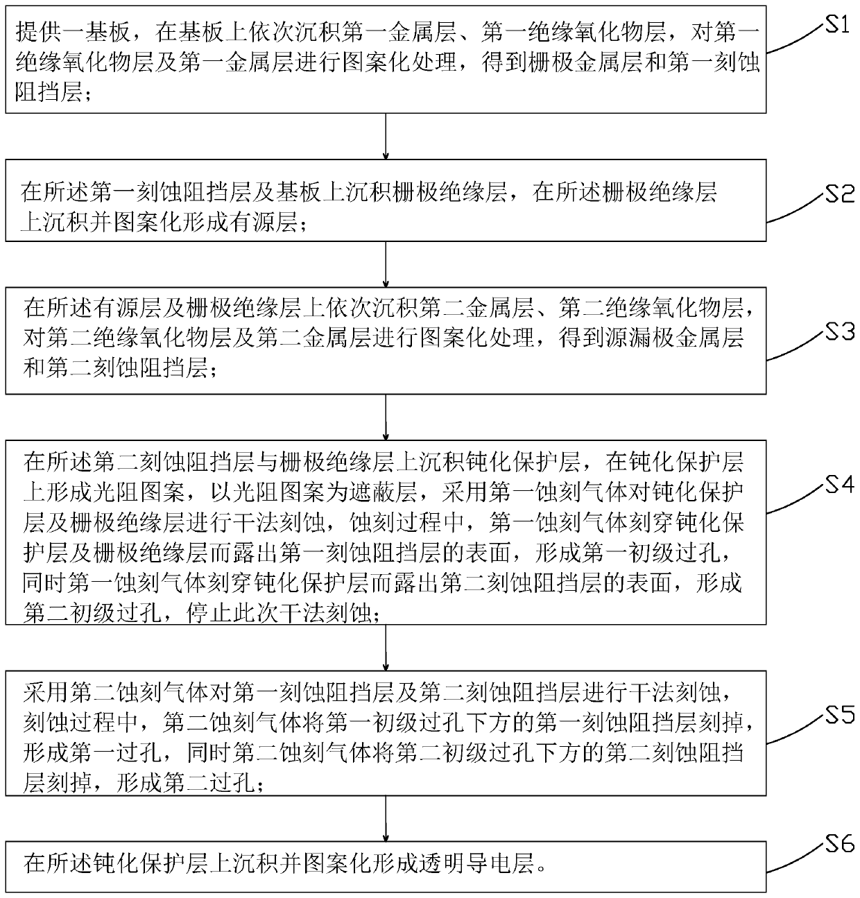
[0037] see figure 2 , the present invention provides a method for manufacturing a bottom-gate TFT substrate, comprising the following steps:

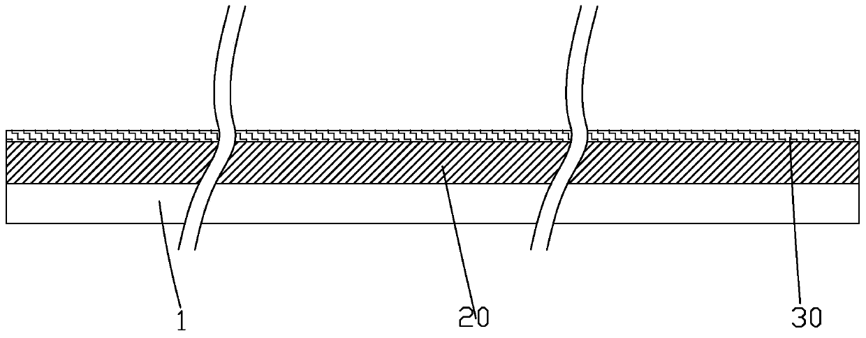
[0038] Step S1, such as Figure 3-4 As shown, a substrate 1 is provided, and a first metal layer 20 is sequentially deposited on the substrate 1 by physical vapor deposition (Physical Vapor Deposition, PVD), by physical vapor deposition or atomic layer deposition (Atomic layer deposition, ALD) Deposit the first insulating oxide layer 30, then pattern the first insulating oxide layer 30 and the first metal layer 20, obtain the gate metal layer 2 from the first metal layer 20, and form the first insulating oxide layer 30 The first etching stopper layer 3 having the same pattern and shape as the gate met...


PUM


Abstract

The invention provides a method for manufacturing a bottom-gate TFT (Thin Film Transistor) substrate, which comprises the steps of forming a first etching barrier layer on a gate metal layer, and forming a second etching barrier layer on a source-drain metal layer; when via holes are formed respectively above the gate metal layer and the source-drain metal layer, firstly etching to the first etching barrier layer and the second etching barrier layer by adopting a first etching gas, forming a first primary via hole and a second primary via hole respectively above the gate metal layer and the source-drain metal layer correspondingly, then etching the first etching barrier layer below the first primary via hole and the second etching barrier layer below the second primary via hole simultaneously by adopting a second etching gas, wherein the first etching barrier layer and the second etching barrier layer can be etched through simultaneously because the first etching barrier layer and the second etching barrier layer are of the same material and thickness, thereby forming a first via hole above the gate metal layer and a second via hole above the source-drain metal layer synchronously, and avoiding source-drain contact resistance and line connection from being affected by serious over-etching of the source-drain metal layer.

Description

technical field [0001] The invention relates to the field of display technology, in particular to a method for manufacturing a bottom-gate TFT substrate. Background technique [0002] Thin Film Transistor (TFT for short) is currently the main component in Liquid Crystal Display (LCD for short) and Active Matrix / Organic Light-Emitting Diode (AMOLED for short) The driving element is directly related to the development direction of the high-performance flat panel display device. Therefore, whether it is an LCD display panel or an AMOLED display panel, it usually has a TFT substrate. Taking the LCD display panel as an example, it is mainly composed of a TFT substrate, a color filter (Color Filter, CF) substrate, and a liquid crystal layer (Liquid Crystal Layer) arranged between the two substrates. Its working principle is The rotation of the liquid crystal molecules in the liquid crystal layer is controlled by applying a driving voltage on the TFT substrate and the CF substrat...

Claims


Application Information

Patent Timeline
Patent Type & Authority Patents(China)
IPC IPC(8): H01L27/12
CPCH01L27/1259H01L27/1288
Inventor 何敏博
Owner TCL CHINA STAR OPTOELECTRONICS TECH CO LTD
Learn More