Photoelectric detector with mesh-shaped perovskite nanowires and fabrication method of photoelectric detector

A photodetector and perovskite technology, applied in the direction of nanotechnology, photovoltaic power generation, nanotechnology, etc., can solve the problems that restrict the practical application of perovskite materials, instability, decomposition failure, etc., to improve the performance and use of light detection Long life, low cost, and the effect of increasing air life

Inactive Publication Date: 2017-11-03
YANGTZE UNIVERSITY
View PDF3 Cites 8 Cited by
  • Summary
  • Abstract
  • Description
  • Claims
  • Application Information

AI Technical Summary

Problems solved by technology

Although perovskite is regarded as a potential next-generation solar cell material, it is unstable in the air and easily reacts with moisture and oxygen in the air to decompose and fail, which greatly restricts the development of perovskite materials. practical application

Method used


Image

  • Photoelectric detector with mesh-shaped perovskite nanowires and fabrication method of photoelectric detector
  • Photoelectric detector with mesh-shaped perovskite nanowires and fabrication method of photoelectric detector
  • Photoelectric detector with mesh-shaped perovskite nanowires and fabrication method of photoelectric detector

Examples


Embodiment 1

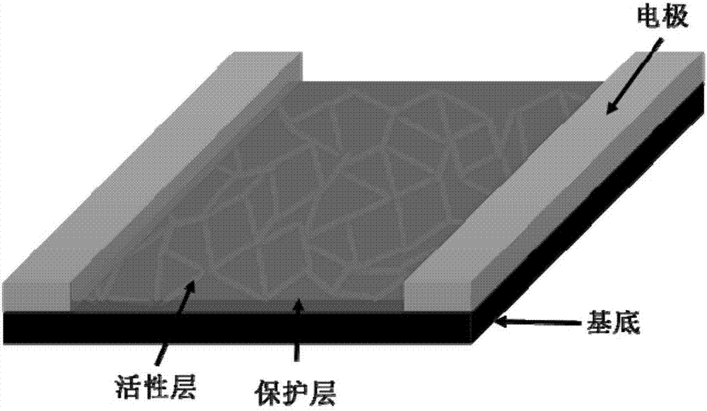
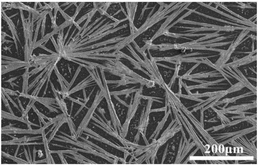
[0036] This embodiment provides a photodetector with mesh-like perovskite nanowires, the schematic diagram of which is shown in the attached figure 1 As shown, it includes a base, a protective layer, an absorbing layer, and an electrode. Electrodes are respectively arranged on both sides of the upper surface of the base, and a protective layer and an absorbing layer are arranged on the upper surface of the base between the two electrodes; the protective layer is thermoplastic Acrylic resin film, the absorption layer is a network structure film formed by interlacing perovskite nanowires, the surface of the perovskite nanowires is wrapped by acrylic resin, and the perovskite is CH 3 NH 3 Pb I 3 .

[0037] The preparation method of the photodetector with mesh perovskite nanowires in this embodiment comprises the following steps:

[0038] (1) Use deionized water, acetone, and absolute ethanol to ultrasonically clean the substrate, then dry it with high-purity gas, and finally t...

Embodiment 2

[0047] This embodiment provides a photodetector with mesh-like perovskite nanowires, the schematic diagram of which is shown in the attached figure 1 As shown, it includes a base, a protective layer, an absorbing layer, and an electrode. Electrodes are respectively arranged on both sides of the upper surface of the base, and a protective layer and an absorbing layer are arranged on the upper surface of the base between the two electrodes; the protective layer is thermoplastic Acrylic resin film, the absorption layer is a network structure film formed by interlacing perovskite nanowires, the surface of the perovskite nanowires is wrapped by acrylic resin, and the perovskite is CH 3 NH 3 PbBr 3 .

[0048] The preparation method of the photodetector with mesh perovskite nanowires in this embodiment comprises the following steps:

[0049] (1) Use deionized water, acetone, and absolute ethanol to ultrasonically clean the substrate, then dry it with high-purity gas, and finally t...

Embodiment 3

[0058] This embodiment provides a photodetector with mesh-like perovskite nanowires, the schematic diagram of which is shown in the attached figure 1 As shown, it includes a base, a protective layer, an absorbing layer, and an electrode. Electrodes are respectively arranged on both sides of the upper surface of the base, and a protective layer and an absorbing layer are arranged on the upper surface of the base between the two electrodes; the protective layer is thermoplastic Acrylic resin film, the absorption layer is a network structure film formed by interlacing perovskite nanowires, the surface of the perovskite nanowires is wrapped by acrylic resin, and the perovskite is CH 3 NH 3 PbCl 3 .

[0059] The preparation method of the photodetector with mesh perovskite nanowires in this embodiment comprises the following steps:

[0060] (1) Use deionized water, acetone, and absolute ethanol to ultrasonically clean the substrate, then dry it with high-purity gas, and finally t...


PUM


Abstract

The invention provides a photoelectric detector with mesh-shaped perovskite nanowires. The photoelectric detector comprises a substrate, a protection layer, an absorption layer and electrodes, wherein the electrodes are respectively arranged at two sides of an upper surface of the substrate, the protection layer and the absorption layer are arranged between the two electrodes arranged on the upper surface of the substrate, the protection layer is a thermoplastic acrylic resin, the absorption layer is a meshed structure thin film formed by arranging the perovskite nanowires in a staggered way, and surfaces of the perovskite nanowires are wrapped by acrylic resin. Moreover, the invention provides a fabrication method of the photoelectric detector. The photoelectric detector has the advantages of excellent performance, stable performance in air, simple technological process, good product performance and low cost.

Description

technical field [0001] The invention relates to the technical field of optoelectronic devices, in particular to a photodetector with mesh perovskite nanowires and a preparation method thereof. Background technique [0002] Optical signal detection is an important part of spectral measurement. Photodetectors can convert light radiation energy into current or voltage signals for measurement. They are the most commonly used optical signal detectors. They are used in ray measurement and detection, industrial automatic control, photometric missile guidance, infrared thermal imaging, infrared remote sensing, etc. has wide application. Therefore, the development of photodetectors with good performance and low cost is of great significance to the development of the optoelectronic field. [0003] Recently, a perovskite-based structure (CH 3 NH 3 PbA 3 or CH 3 NH 3 PbA 3-x B x , A, B=I, Cl, Br) materials have attracted widespread attention in the field of optoelectronics. Be...

Claims


Application Information

Patent Timeline
IPC IPC(8): H01L51/46H01L51/42H01L51/44H01L51/48B82Y30/00B82Y40/00
CPCB82Y30/00B82Y40/00H10K71/12H10K85/30H10K30/30H10K30/88Y02E10/549Y02P70/50
Inventor 程书博刘孟思陈善俊
Owner YANGTZE UNIVERSITY
Why Eureka
Try Eureka