

Perovskite nanowire array photoelectric detector and preparation method thereof
A nanowire array, photodetector technology, applied in nanotechnology, photovoltaic power generation, nanotechnology and other directions, can solve the problems of perovskite materials such as fear of water, degradation of stability and performance, etc.
- Summary
- Abstract
- Description
- Claims
- Application Information
AI Technical Summary
Problems solved by technology
Method used
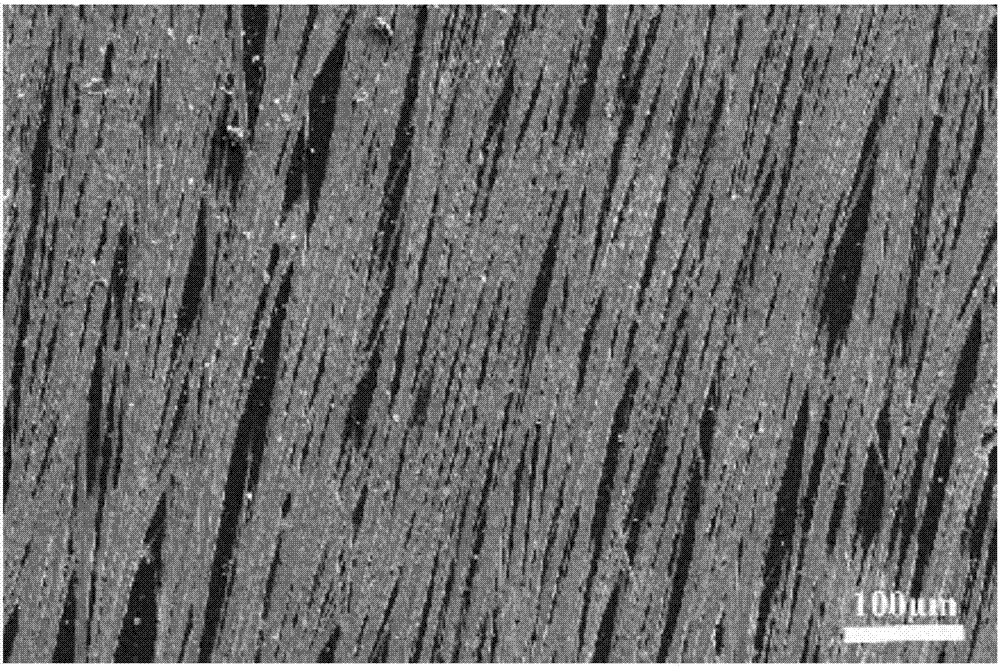
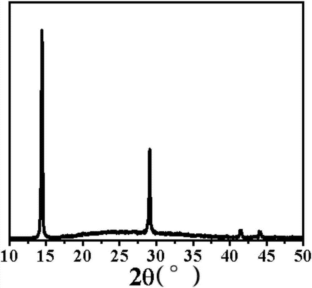
Image

Examples
Embodiment 1
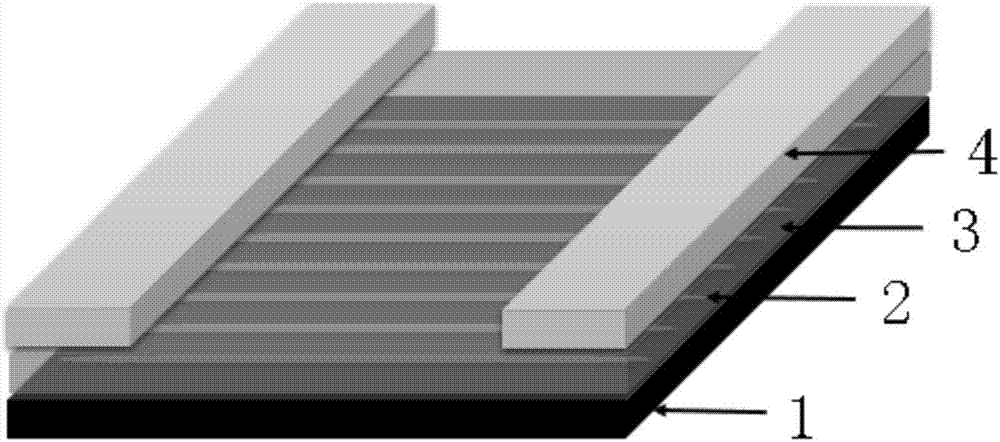
[0039] An embodiment of the perovskite nanowire array photodetector and its preparation method of the present invention. The structure of the perovskite nanowire array photodetector is as follows: figure 1 shown. Depend on figure 1 It can be seen that it mainly includes a substrate 1, an organic-inorganic hybrid perovskite nanowire array 2 compounded on the upper surface of the substrate 1, and a 4,4'-cyclohexyl disulfide covering the organic-inorganic hybrid perovskite nanowire array 2. [N,N-bis(4-methylphenyl)aniline] protective layer 3 and composite on 4,4'-cyclohexyl bis[N,N-bis(4-methylphenyl)aniline] protective layer 3 Surface electrodes 4. Wherein, the substrate 1 is a glass sheet with a surface roughness (Ra) of 8nm, and a 4,4'-cyclohexylbis[N,N-bis(4-methylphenyl)aniline] protective layer 3 with a thickness of 45nm.
[0040] The preparation method of the perovskite nanowire array photodetector comprises the following steps:
[0041] (1) Substrate 1 was ultrasonic...
Embodiment 2
[0050] An embodiment of the perovskite nanowire array photodetector and its preparation method of the present invention. The structure of the perovskite nanowire array photodetector is as follows: figure 1 shown. Depend on figure 1It can be seen that it mainly includes a substrate 1, an organic-inorganic hybrid perovskite nanowire array 2 compounded on the upper surface of the substrate 1, and a 4,4'-cyclohexyl disulfide covering the organic-inorganic hybrid perovskite nanowire array 2. [N,N-bis(4-methylphenyl)aniline] protective layer 3 and composite on 4,4'-cyclohexyl bis[N,N-bis(4-methylphenyl)aniline] protective layer 3 Surface electrodes 4. Wherein, the substrate 1 is a quartz plate with a surface roughness (Ra) of 10 nm, and a 4,4'-cyclohexylbis[N,N-bis(4-methylphenyl)aniline] protective layer 3 with a thickness of 50 nm.
[0051] The preparation method of the perovskite nanowire array photodetector comprises the following steps:
[0052] (1) Substrate 1 was ultraso...
Embodiment 3
[0060] An embodiment of the perovskite nanowire array photodetector and its preparation method of the present invention. The structure of the perovskite nanowire array photodetector is as follows: figure 1 shown. Depend on figure 1 It can be seen that it mainly includes a substrate 1, an organic-inorganic hybrid perovskite nanowire array 2 compounded on the upper surface of the substrate 1, and a 4,4'-cyclohexyl disulfide covering the organic-inorganic hybrid perovskite nanowire array 2. [N,N-bis(4-methylphenyl)aniline] protective layer 3 and composite on 4,4'-cyclohexyl bis[N,N-bis(4-methylphenyl)aniline] protective layer 3 Surface electrodes 4. Among them, substrate 1 is polyethylene terephthalate (PET), its surface roughness (Ra) is 9nm, 4,4'-cyclohexylbis[N,N-bis(4-methylphenyl) Aniline] protective layer 3 had a thickness of 30 nm.
[0061] The preparation method of the perovskite nanowire array photodetector comprises the following steps:
[0062] (1) Substrate 1 wa...
PUM
| Property | Measurement | Unit |
|---|---|---|
| Thickness | aaaaa | aaaaa |
| Surface roughness | aaaaa | aaaaa |
| Surface roughness | aaaaa | aaaaa |
Abstract
Description
Claims
Application Information