Single-sided light emission light emitting element and production method thereof

A technology for light-emitting components and single-sided light emission, which is applied to electrical components, semiconductor devices, circuits, etc., can solve problems such as abnormal module performance and appearance, and low design flexibility, so as to achieve improved photoelectric characteristics, good competitive advantages, and light emission direction strong effect

Active Publication Date: 2016-10-12
YANGZHOU ZHONGKE SEMICON LIGHTING
View PDF4 Cites 12 Cited by
  • Summary
  • Abstract
  • Description
  • Claims
  • Application Information

AI Technical Summary

Problems solved by technology

However, the overall printing requires the use of high-precision cutting equipment to obtain a single chip-scale packaged LED product. The external dimensions of the product obtained by module printing are fixed, and the design flexibility is small during application. The failure of any LED in the module will lead to poor performance of the module. abnormal appearance

Method used


Image

  • Single-sided light emission light emitting element and production method thereof
  • Single-sided light emission light emitting element and production method thereof
  • Single-sided light emission light emitting element and production method thereof

Examples


1 example 1

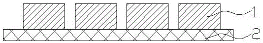
[0026] 1. Fix a plurality of light-emitting diodes 1 on the same surface of the fixing film 2 in an array with equal row and column spacing. Such as figure 1 Shown.

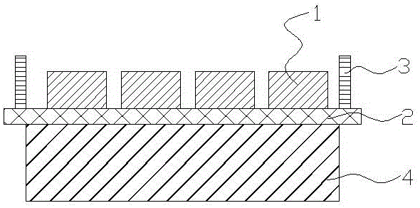
[0027] 2. Position the fixed film 2 tightly on the carrier 4 through the clamp 3, and make each light-emitting diode 1 face upwards, such as figure 2 Shown.

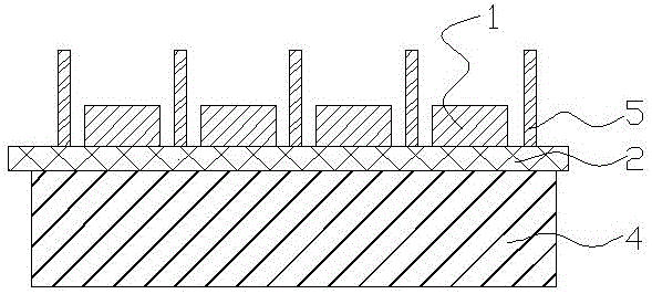
[0028] 3. Fix the steel mesh 5 on the fixing film 2, and use optical positioning components to make the light-emitting diodes 1 in the middle of each mesh of the steel mesh 5 one by one. Note: The mesh depth of the steel mesh 5 is slightly larger than the thickness of the light emitting diode 1. Such as image 3 Shown.

[0029] Use a spatula to fill the reflective glue 6 in each mesh of the steel mesh 5, such as Figure 4 Shown. After the reflective adhesive 6 is dried, it is separated from the steel mesh 5, and the reflective adhesive on the light-emitting surface of the light-emitting diode 1 is removed by grinding to obtain a semi-product such as Figure 5...

2 example 2

[0037] Others are similar, except that when designing the steel mesh 5, the mesh is designed into a bell mouth shape with an upper surface area larger than a lower surface area.

[0038] As a result, products such as Picture 8 Shown:

[0039] Two electrodes 8 are arranged on the bottom surface of the light-emitting diode 1, a phosphor glue layer 7 is arranged on the front surface of the light-emitting diode 1, and a reflective glue layer 6 is arranged on all four sides of the light-emitting diode 1.

[0040] The thickness of the reflective adhesive layer 6 close to the bottom surface is thinner than that close to the front surface.

[0041] The phosphor glue layer 7 may also be formed by multiple phosphor glue layers with different refractive indexes.


PUM


Abstract

The invention provides a single-sided light emission light emitting element and a production method thereof, and relates to the field of semiconductor device packaging. Two electrodes are arranged at the bottom of a light emitting diode. The single-sided light emission light emitting element is characterized in that a fluorescent powder glue layer is arranged on the front of the light emitting diode, and reflective glue layers are arranged on four sides of the light emitting diode. The preparation method is characterized in that a single single-sided light emitting diode without cutting marks on four sides without cutting is acquired, and the fluorescent powder glue layer of the light emission side of the light emitting diode can be designed through repeated filling. According to the invention, the preparation process does not need expensive and high-precision cutting equipment, so that an enterprise can have more abundant capital to expand production; since cutting is prevented, the utilization ratio of fluorescent powder glue is improved; and production period is shortened.

Description

Technical field [0001] The present invention relates to the field of semiconductor device packaging, and more specifically to the packaging process of white light emitting diode chips. Background technique [0002] Under the market's call for miniaturization and high current density of light-emitting diode devices, chip-scale packaged light-emitting diodes have become the light-emitting diode industry by eliminating redundant structures such as brackets and gold wires, reducing the size, excellent heat dissipation performance, and being able to withstand high-density current. The rising star has attracted the attention of many chip and packaging factories. [0003] However, due to the immature production technology route and high equipment investment costs, there are only a handful of chip-scale packaged light-emitting diode products in the domestic and foreign markets. In order to seize the emerging markets, major domestic and foreign manufacturers have racked their brains to sei...

Claims


Application Information

Patent Timeline
Patent Type & Authority Applications(China)
IPC IPC(8): H01L33/48H01L33/50H01L33/60
CPCH01L33/48H01L33/505H01L33/60H01L2933/0041H01L2933/0058
Inventor 臧传亮王国宏李银川金豫浙孙一军李志聪章加奇张应吴杰
Owner YANGZHOU ZHONGKE SEMICON LIGHTING
Why Eureka
Try Eureka