Touch panel and manufacturing method thereof

a technology of touch panel and manufacturing method, which is applied in the field of touch panel, can solve the problems of insufficient flexibility and challenge to certain properties of metal oxide film, and achieve the effects of low circuit impedance, good optical and electrical characteristics of display area, and high manufacturing efficiency

Active Publication Date: 2020-09-24
CAMBRIOS FILM SOLUTIONS CORP
View PDF0 Cites 12 Cited by
  • Summary
  • Abstract
  • Description
  • Claims
  • Application Information

AI Technical Summary

Benefits of technology

[0007]In some embodiments of the present disclosure, a method for manufacturing a touch panel is proposed, which has the advantag

Problems solved by technology

However, certain properties of these metal oxide films

Method used


Image

  • Touch panel and manufacturing method thereof
  • Touch panel and manufacturing method thereof
  • Touch panel and manufacturing method thereof

Examples


Embodiment Construction

[0038]The various embodiments of the present disclosure are disclosed in the drawings. However, it should be understood that these practical details are not intended to limit the invention. That is, in some embodiments of the invention, these practical details are not necessary. In addition, some of the conventional structures and elements are shown in the drawings in a simplified manner.

[0039]The terms “about”, “approximately” or “substantially” used herein generally refer to the error or range of values is within 20%, preferably within 10%, and more preferably within 5%. Unless otherwise stated, the numerical values mentioned are considered as approximations. That is, they have an error or range as indicated by “about” or “rough”. In addition, the terms “pattern”, “graphic” as used herein mean the same or similar meanings, and for convenience of explanation, the terms may be used interchangeably.

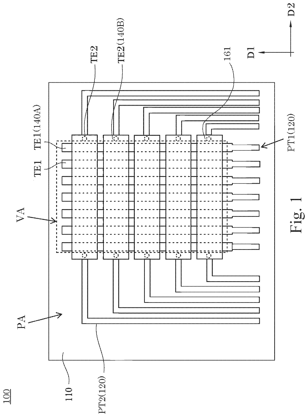
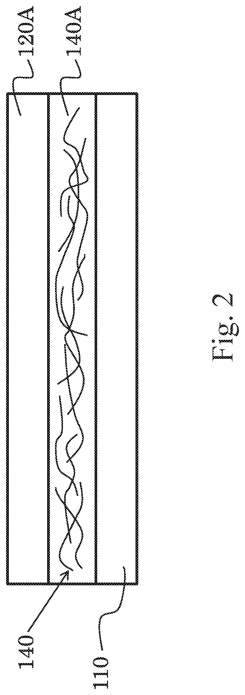
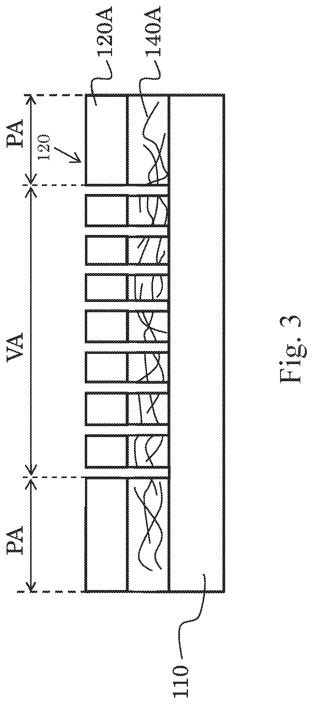
[0040]A touch panel 100 in accordance with various embodiments is shown in FIG. 1. The...


PUM


Abstract

A touch panel includes a substrate, first and second touch sensing electrodes, and first and second traces. The substrate includes a display area and a peripheral area. The first and second touch sensing electrodes are formed on the display area, and the first and second traces are formed on the peripheral area. The first touch sensing electrode is formed by a first portion of a metal nanowire layer, which is patterned. The peripheral trace includes a conductive layer and a second portion of the metal nanowire layer, both of which are patterned in a co-etch step. The conductive layer and the second portion of the metal nanowire layer have a coplanar etched surface. The second touch sensing electrode is formed on an insulating layer and connects with the second trace.

Description

CROSS-REFERENCE TO RELATED APPLICATION[0001]This application claims priority to China Application Serial Number 201910223160.5, filed Mar. 22, 2019, which is herein incorporated by reference.BACKGROUNDTechnology Field[0002]This disclosure relates to a touch panel and a manufacturing method thereof.Description of Related Art[0003]Transparent conductive materials, which have good light transmission and electrical conductivity, are generally applied to devices related to display panels or touch panels. Transparent conductive materials include metal oxides, such as indium tin oxide (ITO), indium zinc oxide (IZO), cadmium tin oxide (CTO) or aluminum-doped zinc oxide (AZO). However, certain properties of these metal oxide films have been challenged, such as insufficient flexibility. In some cases, patterning of the metal oxide film may also be readily visible to the user. Therefore, various transparent conductive materials, including metal nanowires, are being developed currently.[0004]Th...

Claims


Application Information

Patent Timeline
IPC IPC(8): G06F3/041G06F3/047
CPCG06F3/04142G06F3/047G06F3/0412G06F2203/04103G06F3/04164G06F3/0445G06F3/0446G02F1/13338G02F1/1335G06F3/041
Inventor HSIAO, CHUNG-CHINLIEN, SIOU-CHENGHSU, CHENG-YUANYEW, JEN-YULIU, KANG-YUCAO, WEI-NA
Owner CAMBRIOS FILM SOLUTIONS CORP
Why Eureka
Try Eureka