Air socket for testing integrated circuits

a technology of integrated circuits and air sockets, which is applied in the field of testing of semiconductor devices, can solve the problems of inability to temporarily electrically connect, the terminals of electronic components are not co-planar, and the contact bumps on the flip-chips are not usually uniform sizes, so as to improve the probability of a successful chip test, improve manufacturing efficiency and quality control, and improve the electrical connection

Inactive Publication Date: 2006-07-04
MICRON TECH INC
View PDF31 Cites 1 Cited by
  • Summary
  • Abstract
  • Description
  • Claims
  • Application Information

AI Technical Summary

Benefits of technology

[0011]The invention improves the electrical connections that are made between a flip-chip or BOC and a socket during the testing phase of fabrication. The invention can increase manufacturing efficiency and quality control by enabling the testing of flip-chips or BOCs without regard to whether its contact bumps are co-planar or have varying heights or diameters. Rather than using a solid base upon which to attach the contact members, the invention employs a flexible membrane for their attachment to allow relative motion between the contact members. This relative motion, derived from the resiliency of the flexible membrane, allows the contact members on the flexible membrane to adapt to the height variations of the contact bumps so as to form an electrical connection, and thereby improve the probability of a successful test of the chip. These variations may be on the same chip or between multiple chips. The movement of the flexible membrane is permitted by its attachment to a housing with a recess. The recess is covered by the flexible membrane to form a chamber in the housing. The chamber is filled with a fluid material, herein defined as a liquid or gas, which may form a delta between the chamber pressure and ambient pressure at a steady state (i.e. pressurized), be sealed at ambient pressure at a steady state, or be open to ambient pressure during the test sequence. The contact members are electrically connected by way of electrical contacts to the test equipment to maintain the flexibility of the flexible membrane.

Problems solved by technology

A subtle problem often associated with the temporary interconnection of electrical components for testing is that the terminals of an electronic component are not co-planar.
The contact bumps on the flip-chip are not usually a uniform size because of the imprecise solidifying characteristics of the conductive materials used in creating the contact bumps.
Accordingly, since the contact bumps may not be of a uniform shape, it may not be possible to temporarily electrically connect each of them to the socket during a test sequence.
Nevertheless, the bumps on the flip-chip are not reflowed to achieve a connection to the socket during testing, as this connection is only temporary and would lead to the loss of the contact bumps or at least their significant degradation.
Furthermore, the process of reflowing contact bumps requires the addition of thermal energy to the coupled electrical components which can adversely affect not only the integrated circuit contained in the component, but also the test socket.
Thus, the inability to achieve an electrical connection between all of the solder bumps and the socket prevents an accurate test from being conducted, and may lead to the discarding of an otherwise usable flip-chip.

Method used


Image

  • Air socket for testing integrated circuits
  • Air socket for testing integrated circuits
  • Air socket for testing integrated circuits

Examples


Embodiment Construction

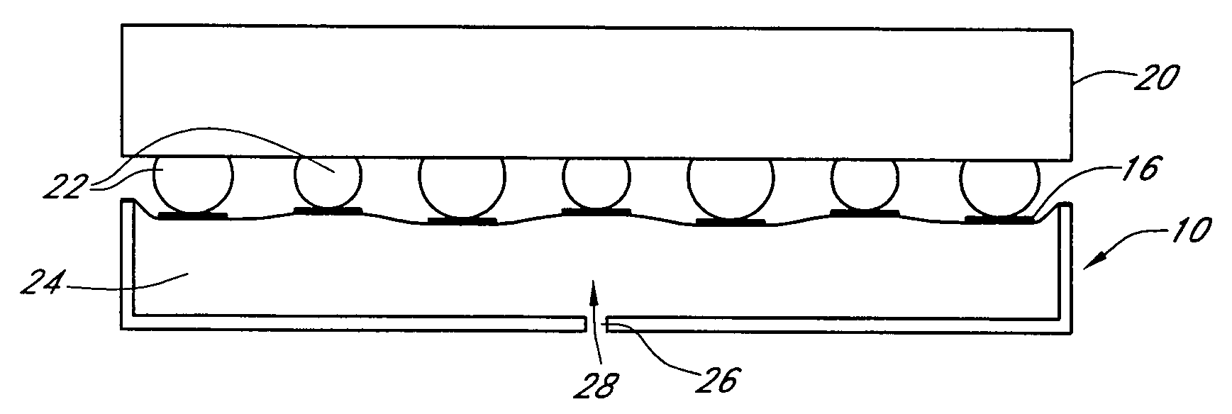
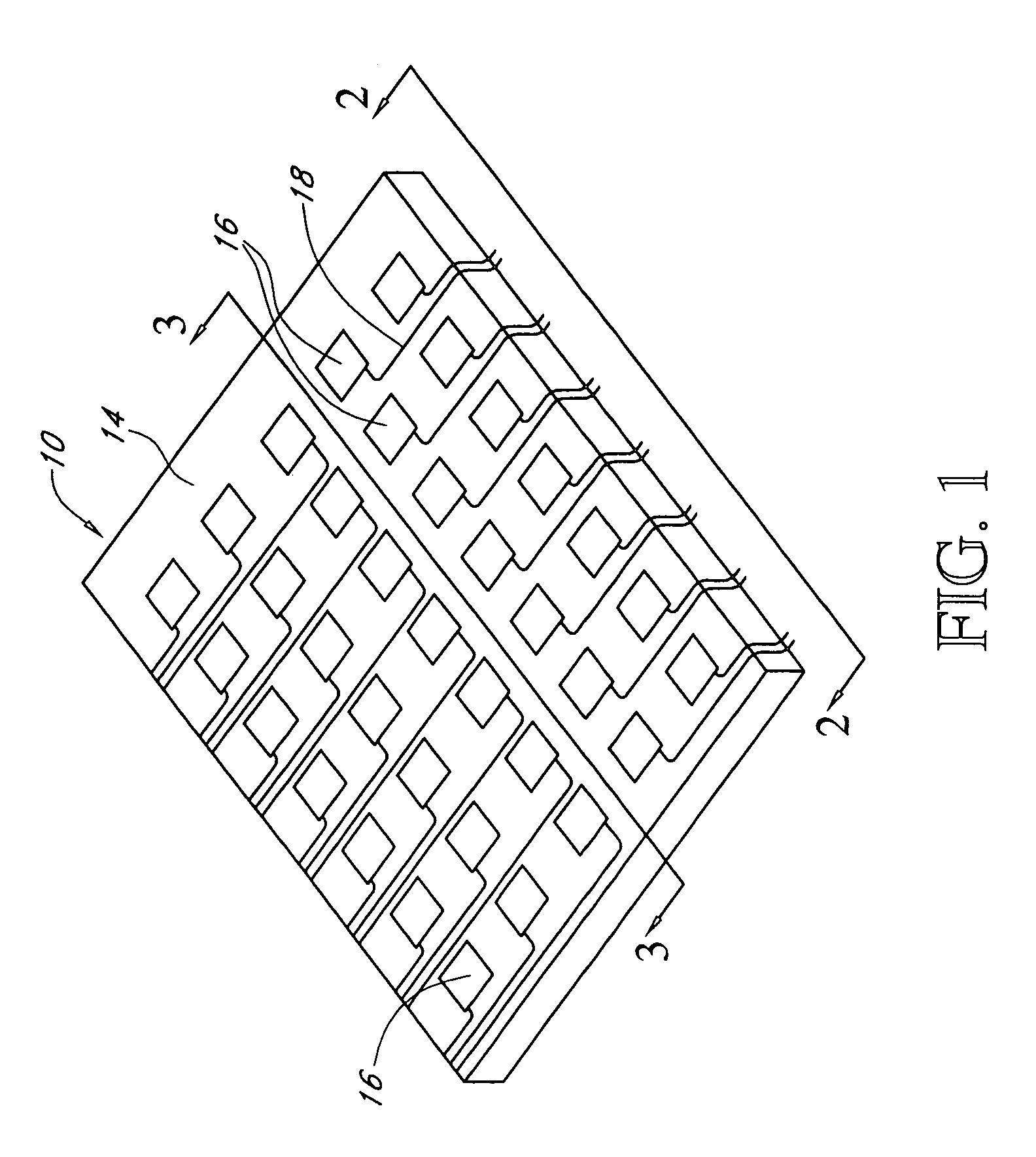
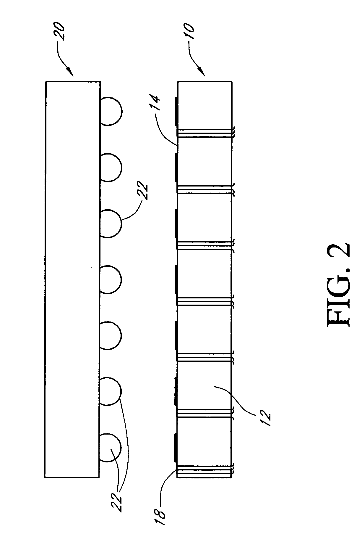
[0026]Broadly stated, FIG. 1 shows an overview of an embodiment of an adjustable membrane test device for a semiconductor. FIG. 1 is a perspective view of a socket 10 of a preferred embodiment of the invention. The socket 10 consists of a housing 12 with a recess (not shown) covered on at least one side with a flexible membrane 14 to form a chamber (not shown) in the housing 12. The housing 12 is rigidly designed to provide the support for the attached flexible membrane 14. The flexible membrane 14 is made from a non-conductive material and creates an adjustable surface.

[0027]A plurality of contact members 16 are attached to that surface of the flexible membrane 14 which faces the electrical device under test. The plurality of contact members 16 may take the form of individual planar surfaces such as those shown or, alternatively, concave surfaces, convex surfaces, linear protrusions such as piercing contacts, dendrite protrusions or other geometric structures configured to make ind...


PUM

PropertyMeasurementUnit
temperaturesaaaaaaaaaa
flexibleaaaaaaaaaa
depthaaaaaaaaaa

Abstract

An electrical component testing device comprising a housing having at least one recess covered by a flexible membrane so as to form a chamber. A fluid passage extends through a portion of the housing and connects to the chamber thus permitting passage of a fluid material into the chamber. At least one contact member is positioned on the flexible membrane so as to provide an electrical connection to an electrical contact on a device to be tested.

Description

CROSS-REFERENCE TO RELATED CO-PENDING APPLICATION[0001]This application is a divisional of U.S. patent application Ser. No. 09 / 653,111, filed Aug. 31, 2000 now U.S. Pat. No. 6,690,184, entitled “AIR SOCKET FOR TESTING INTEGRATED CIRCUITS,” which is incorporated herein by reference.BACKGROUND OF THE INVENTION[0002]1. Field of the Invention[0003]The invention relates to the testing of semiconductor devices. More specifically, the invention relates to a method and apparatus for improving the electrical connections during a testing sequence.[0004]2. Description of the Related Art[0005]Flip-chip and bumped die technology is well known in the art. A flip-chip or bumped die is a semiconductor chip having contact bumps, typically in the form of spherical solder balls or controlled collapse chip connector (C4s) balls, which are electrically connected to the I / O contacts, or contact pads, formed on the active circuit or front side thereof. The I / O contacts provide signal, power, and ground co...

Claims


Application Information

Patent Timeline
Patent Type & Authority Patents(United States)
IPC IPC(8): G01R3/00G01R1/04
CPCG01R1/0483G01R3/00G01R1/0735H01R13/24Y10T29/49147Y10T29/49117Y10T29/49169Y10T29/49165Y10T29/4913Y10T29/49002Y10T29/49007
Inventor AKRAM, SALMAN
Owner MICRON TECH INC
Why Eureka
Try Eureka