Method of designing, fabricating, testing and interconnecting an IC to external circuit nodes

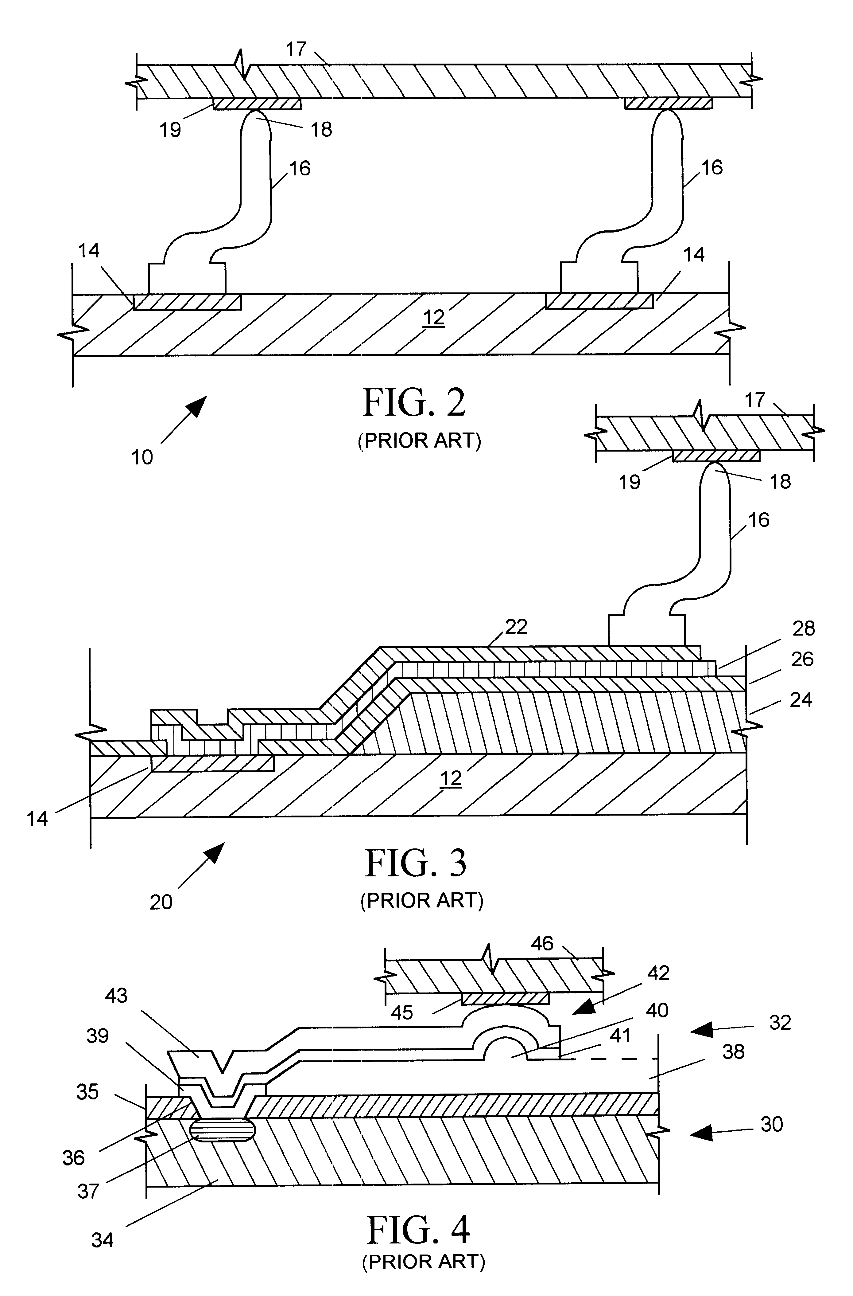
a technology of external circuit node and design, applied in the direction of instruments, program control, waveguide type devices, etc., can solve the problems of inability to verify the timing of the circuit, the interconnect system can severely attenuate and distort the signals passing between the ic and external circuit, and the timing verification at this stage of the design may not be entirely accurate, so as to facilitate the optimization of the testing and operating environmen

Inactive Publication Date: 2003-03-25
FORMFACTOR INC
View PDF4 Cites 209 Cited by
  • Summary
  • Abstract
  • Description
  • Claims
  • Application Information

AI Technical Summary

Benefits of technology

to provide a system for designing, simulating, verifying, fabricating and testing an IC that permits a designer to easily optimize the testing and operating environment interconnect system for each IC terminal to suit the characteristics of the particular signal it is to convey.

Problems solved by technology

Since the HDL model is a relatively high level behavioral model of the circuit, simulation can verify circuit logic at step 404 but cannot verify circuit timing because it does not take into account various constraints of the particular semiconductor technology that will implement the IC.
However, timing constraints verification at this stage of the design may not be entirely accurate since the netlist model does not specify the actual physical positions on an IC chip of the cells that will form the circuit or the actual lengths and impedance characteristics of signal paths between those cells.
In high frequency applications an interconnect system can severely attenuate and distort signals passing between the IC and external circuits.
However, while minimizing interconnect system inductance and capacitances can help improve bandwidth, flatten frequency response and reduce signal distortion, it is not possible to completely eliminate interconnect system inductance and capacitance.
Thus some level of signal distortion and attenuation in an interconnect system is inevitable, and can become problematic particularly at high signal frequencies.
However, such cell libraries do not include models of the portions of the interconnect system external to an IC such as bond wires and package legs, litho-spring or wire-spring contacts, microstrip traces, circuit board vias and the like because they are not part of the IC.
IC designers typically specify uniform interconnect systems for all IC terminals partly because IC manufacturing processes readily lend themselves to interconnect uniformity and partly because it is difficult and time-consuming to custom design an interconnect system for each IC terminal.
However, while interconnect systems for all terminals of an IC are usually standardized, the frequency response and current-carrying capability of the standard interconnect system may not be ideally suited for all of the IC's I / O, power or ground signals since not all such signals are similar in nature.
Thus, if we use the same interconnect system for each kind of signal, the interconnect system can be a limiting factor in IC design.
When we employ such measures to avoid customizing interconnect systems for individual IC terminals we can increase both the size and cost of an IC.
As I / O signal frequencies increase, the design of structures we use to link a wafer-level IC tester to test points on an IC wafer becomes increasingly problematic.
When wafer-level IC tester interconnect systems do not have the same frequency response characteristics as interconnect systems employed in an IC's intended operating environment, then many ICs that would operate properly in their intended operating environment can fail tests and be rejected or de-rated.
One difficulty in conforming test and operating environment interconnects arises because IC I / O signals typically must travel longer distances in a test environment than in its intended operating environment. FIG. 5 is a simplified side elevation view of a typical wafer-level IC tester 90 that can carry out a memory test at step 428 of FIG. 1 or a logic or parametric test on an IC while still in wafer from.
Such discrepancies between an interconnect system's behavioral model employed during the IC design phase and its actual test and operating environment implementation can cause ICs that would function properly in their intended operating environments to fail tests and be discarded or de-rated.
However high frequency ICs are often tested after they are packaged (as illustrated in FIG. 1) because the wafer-level test environment fails to account for the influence of the bond wires and package legs on IC performance.

Method used


Image

  • Method of designing, fabricating, testing and interconnecting an IC to external circuit nodes
  • Method of designing, fabricating, testing and interconnecting an IC to external circuit nodes
  • Method of designing, fabricating, testing and interconnecting an IC to external circuit nodes

Examples


Embodiment Construction

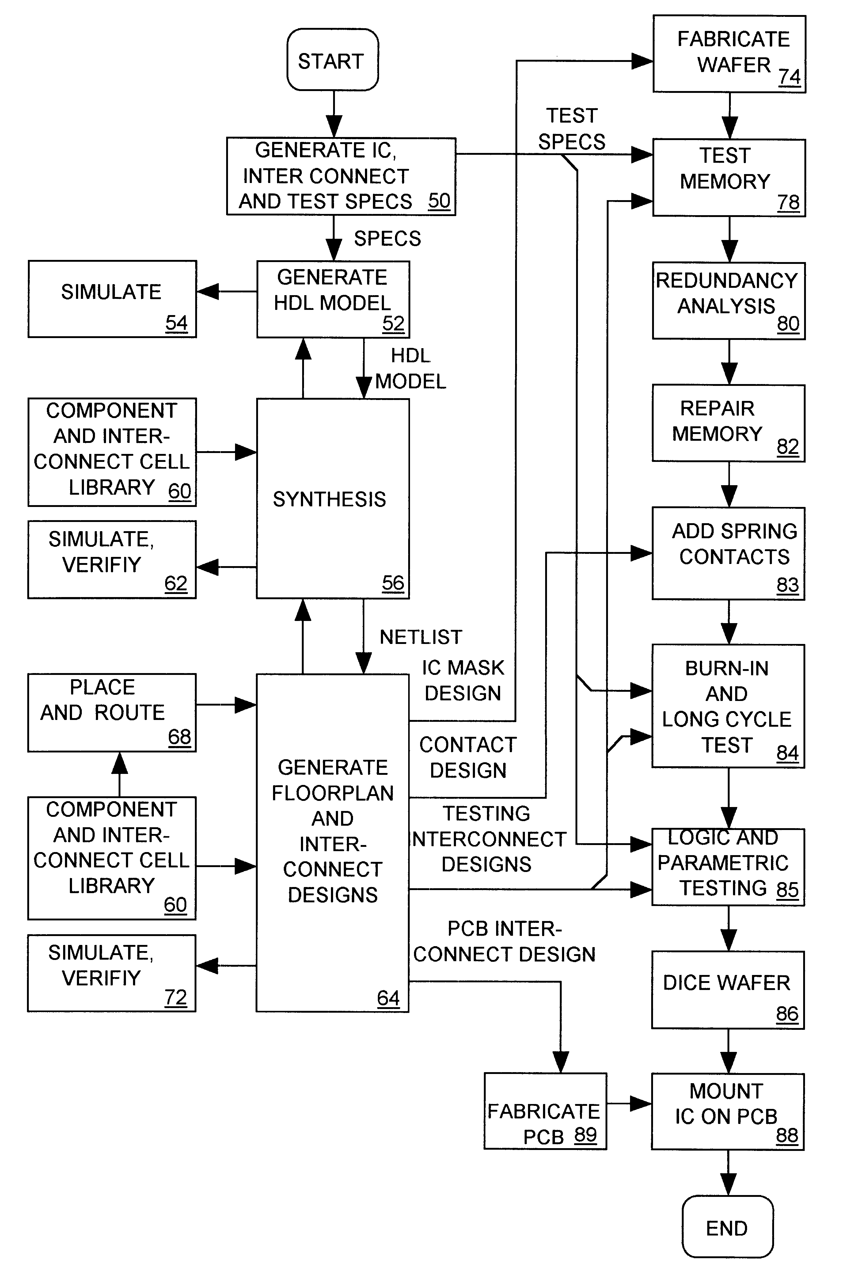
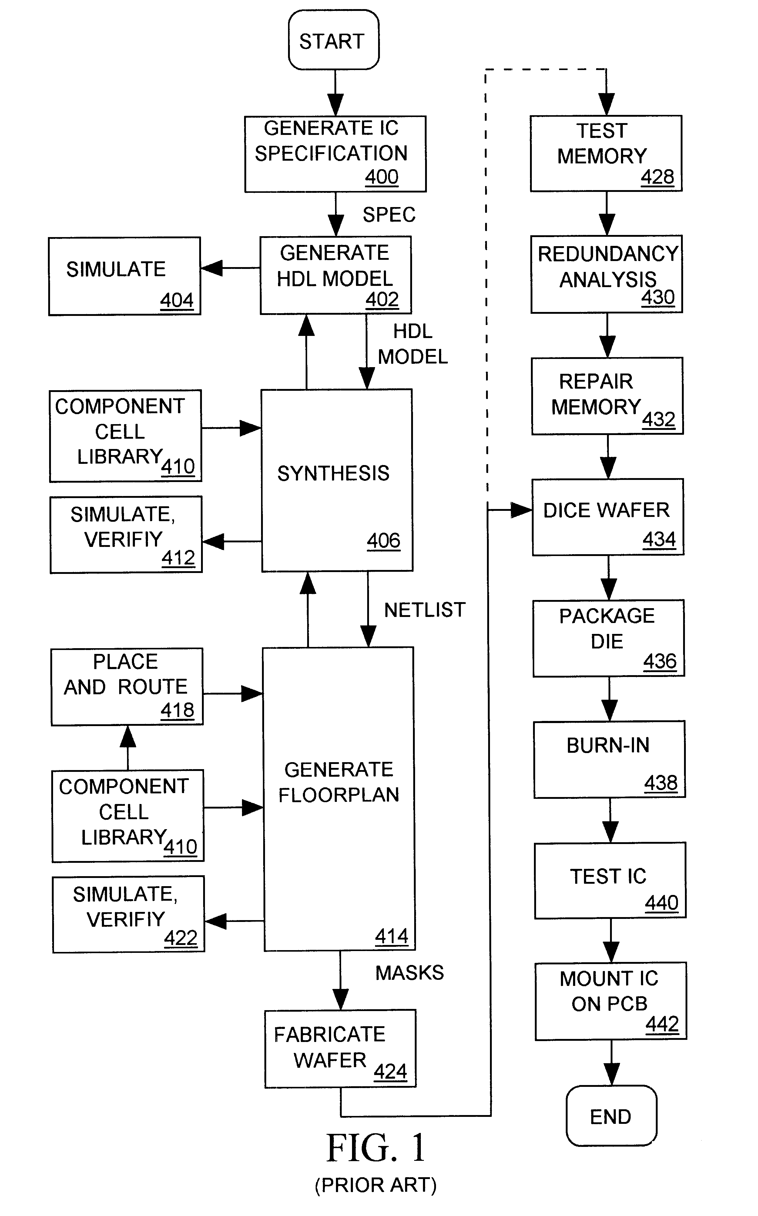
IC Design Using Component Cell Libraries

An integrated circuit (IC) design engineer initially generates a high-level behavioral model of a circuit using a hardware description language (HDL). For a digital IC employing synchronous logic, this model typically describes how the circuit logically processes data flowing between clocked registers. The HDL circuit model is purely logical and does not take into account timing or other limitations of the IC technology that is to implement the IC. However conventional computer-based design (CAD) synthesis tools enable the design engineer to convert the HDL model of the circuit into a lower-level behavioral model (e.g. a "netlist") depicting the circuit as a set of interconnected circuit components or "cells" that may be implemented using a particular IC technology. While the netlist model describes each cell in terms of its behavior rather than its structure, the behavioral model of each cell is based on the known performance of a circuit com...


PUM


Abstract

A method for designing integrated circuits (ICs) and their interconnect systems includes IC component cells and interconnect component cells in a cell library. Each IC component cell provides both a physical and behavioral model of a component that may be incorporated into the IC while each interconnect component cell includes both a physical and behavioral model of a separate internal or external component of an interconnect system that may link the IC to external nodes. Both the IC and its interconnect systems are designed by selecting and specifying interconnections between component cells included in the cell library. Interconnect systems are flexibily designed to act like filters tuned to optimize desired frequency response characteristics. Behavior models of the IC and its interconnect systems, based on the behavior models of their selected component, are subjected to simulation and verification tools to determine whether the IC and its interconnect systems meet various performance criteria and constraints. The structural models of the interconnect systems developed during the design process guide subsequent fabrication of interconnect systems for both the IC's intended testing and operating environments.

Description

1. Field of the InventionThe present invention relates in general to a process of designing, simulating, fabricating, testing and interconnecting integrated circuits (ICs), and in particular to a method for fully integrating the interconnect systems that are to connect ICs to external circuits into all stages of that process.2. Description of Related ArtIntegrated Circuit Process FlowFIG. 1 illustrates a typical prior art process of designing, fabricating, testing, and connecting an integrated circuit (IC). A design engineer initially develops a design specification (step 400) abstractly describing the functionality and overall architecture of the IC and then develops a high-level hardware description language (HDL) model of the IC describing how data flows between clocked registers and how the design processes that data (step 402). The design engineer also programs a circuit simulator (step 404) to simulate circuit behavior based on the HDL circuit model and may iteratively adjust ...

Claims


Application Information

Patent Timeline
Patent Type & Authority Patents(United States)
IPC IPC(8): H01L23/58H01L23/60H01L23/522H01L23/52
CPCH01L23/5227H01L23/60H01L24/49H01L2924/10253H01L2224/45144H01L2924/014H01L2924/01033H01L2924/01023H01L2223/6611H01L2224/48091H01L2224/4813H01L2224/49113H01L2924/01005H01L2924/01006H01L2924/01014H01L2924/01022H01L2924/01028H01L2924/01039H01L2924/01074H01L2924/01079H01L2924/01083H01L2924/14H01L2924/19041H01L2924/19042H01L2924/19043H01L2924/30105H01L2924/30107H01L2924/3011H01L24/48H01L2924/01019H01L2924/00014H01L2924/00H01L2224/45015H01L2924/30111H01L2924/12042H01L24/45H01L2224/45014H01L2924/00015
Inventor MILLER, CHARLES A.LONG, JOHN M.
Owner FORMFACTOR INC
Why Eureka
Try Eureka