

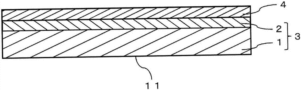
Surface protection adhesive tape for semiconductor wafer backgrinding, and semiconductor wafer grinding method
A technology of grinding and protecting tape, which is applied in the direction of semiconductor devices, semiconductor/solid-state device manufacturing, electric solid-state devices, etc. It can solve the problems that the gap cannot pass through the sensor, the sensor cannot be identified, and the gap cannot be detected to achieve heat resistance. Excellent, improved workability, and improved efficiency
- Summary
- Abstract
- Description
- Claims
- Application Information
AI Technical Summary
Benefits of technology
Problems solved by technology
Method used
Image

Examples
Embodiment 1
[0123] In 100 parts by mass of ethylene-vinyl acetate copolymer (EVA) resin A containing 6.0% by mass of the vinyl acetate component, 0.6 parts by mass of copper phthalocyanine blue containing the blue pigment 5.0% by mass and vinyl acetate were dry blended The content of the ester component is 6.0% by mass of ethylene-vinyl acetate copolymer (EVA) resin B. The extrusion molding was performed by an extrusion molding machine, thereby obtaining a base film A having a thickness of 165 μm and a back surface roughness Rz=1.2 μm.
[0124] Mixing in proportions of 2 mol% of methacrylic acid, 50 mol% of 2-ethylhexyl acrylate, 30 mol% of 2-hydroxyethyl acrylate, and 18 mol% of methyl acrylate, adding 0.2 mass per 100 mass parts of total monomers Parts of azobisisobutyronitrile were copolymerized in an ethyl acetate solution at a temperature of 70°C in a reaction vessel replaced with nitrogen, thereby obtaining a polymer solution with a weight average molecular weight of 800,000. In this ...
Embodiment 2
[0127] In 100 parts by mass of ethylene-vinyl acetate copolymer (EVA) resin A containing 6.0% by mass of the vinyl acetate component, 0.3 parts by mass of copper phthalocyanine blue containing the blue pigment 5.0% by mass and vinyl acetate were dry blended The content of the ester component is 6.0% by mass of ethylene-vinyl acetate copolymer (EVA) resin B. Extrusion molding was performed by an extrusion molding machine, thereby obtaining a base film B having a thickness of 165 μm and a surface roughness of the back surface Rz=0.7 μm.
[0128] Mixing is carried out in a proportion of 1 mol% of methacrylic acid, 22 mol% of 2-hydroxyethyl acrylate, and 77 mol% of butyl acrylate, and 0.3 parts by mass of azobisisobutyronitrile is added to 100 parts by mass of the total monomers. In the reaction vessel replaced with nitrogen, copolymerization was carried out in an ethyl acetate solution at a temperature of 70°C to obtain a polymer solution with a weight average molecular weight of 30...
Embodiment 3
[0131] In 100 parts by mass of ethylene-vinyl acetate copolymer (EVA) resin C having a vinyl acetate content of 10.0% by mass, 0.6 parts by mass of copper phthalocyanine blue containing the blue pigment 5.0% by mass and vinyl acetate were dry blended The content of the ester component is 6.0% by mass of ethylene-vinyl acetate copolymer (EVA) resin B. The extrusion molding was performed by an extrusion molding machine, thereby obtaining a base film C having a thickness of 100 μm and a surface roughness Rz of the back surface Rz=3.7 μm.
[0132] Mixing is carried out in a proportion of 2 mol% methacrylic acid, 29 mol% 2-hydroxyethyl acrylate, and 69 mol% 2-ethylhexyl acrylate, and 0.2 parts by mass of azobisiso is added relative to 100 parts by mass of the total monomers. Nitrile was copolymerized in an ethyl acetate solution in a reaction vessel replaced with nitrogen at a temperature of 70°C to obtain a polymer solution with a weight average molecular weight of 230,000. In this ...
PUM
| Property | Measurement | Unit |
|---|---|---|
| Surface roughness | aaaaa | aaaaa |
| Thickness | aaaaa | aaaaa |
| Melting point | aaaaa | aaaaa |
Abstract
Description
Claims
Application Information