Substrate and manufacturing method, and display panel thereof

A substrate and dam technology, applied in the direction of electrical components, electrical solid devices, circuits, etc., can solve the problem of uneven display

Active Publication Date: 2017-12-08
BOE TECH GRP CO LTD +1
View PDF4 Cites 14 Cited by
  • Summary
  • Abstract
  • Description
  • Claims
  • Application Information

AI Technical Summary

Problems solved by technology

[0005] However, there are also corresponding problems in inkjet printing. Specifically, in order to define the sub-pixel area, it is necessary to make a pixel defining layer before inkjet printing, so that ink droplets of organic materials can smoothly enter the grooves in the sub-pixel area.
However, there is a requirement for the dam of the pixel-defining layer. During inkjet printi

Method used


Image

  • Substrate and manufacturing method, and display panel thereof
  • Substrate and manufacturing method, and display panel thereof
  • Substrate and manufacturing method, and display panel thereof

Examples


Embodiment Construction

[0030] The following will clearly and completely describe the technical solutions in the embodiments of the present invention with reference to the accompanying drawings in the embodiments of the present invention. Obviously, the described embodiments are only some of the embodiments of the present invention, not all of them. Based on the embodiments of the present invention, all other embodiments obtained by persons of ordinary skill in the art without making creative efforts belong to the protection scope of the present invention.

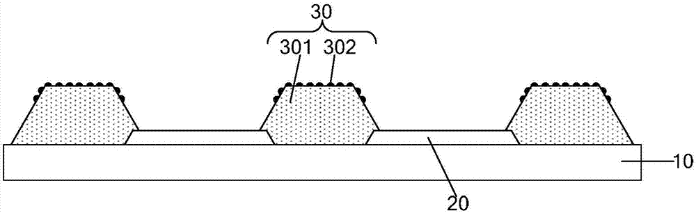
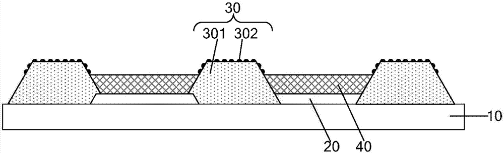
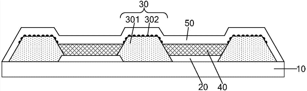
[0031] An embodiment of the present invention provides a substrate, such as figure 1 As shown, it includes a substrate 10, a pixel defining layer 30 disposed on the substrate 10, the pixel defining layer 30 includes a dam 301, and several micron-scale protrusions 302 arranged on the upper surface and side surfaces of the dam 301; the protrusion 302 has lyophobic properties.

[0032] In the present invention, numerous tiny protrusions 302 with ly...


PUM

PropertyMeasurementUnit
Diameteraaaaaaaaaa

Abstract

The embodiments of theinvention provide a substrate and a manufacturing method and display panel thereof, and relates to the technical field of display. The substrate, and the manufacturing and display panel thereof allow even spreading of ink drops in the grooves that are defined by pixel defining layer so as to effectively increase product quality and display effects. The substrate includes a substrate and a pixel defining layer which is disposed on the substrate. The pixel defining layer includes a dam body and a plurality of micrometer-protrusions which are disposed on the supper surface and the lateral of the dam body. The protrusions have lyophobic properties.

Description

technical field [0001] The invention relates to the field of display technology, in particular to a substrate, a preparation method thereof, and a display panel. Background technique [0002] Organic Light Emitting Diode (OLED) display has better contrast ratio, higher brightness, wider viewing angle, wide color gamut and faster refresh rate, and is characterized by its low power consumption and flexible display It is recognized as the next generation display technology. [0003] At present, the organic material functional layer of the OLED display is prepared by vacuum thermal evaporation process, that is, the organic material is heated in a vacuum chamber to sublimate or melt and gasify into a vapor, which is deposited on the substrate through the openings of the metal mask. However, due to the high cost of vacuum thermal evaporation and the difficulty of producing large-scale and fine metal masks, the evaporation process cannot be applied to large-scale substrates. [0...

Claims


Application Information

Patent Timeline
IPC IPC(8): H01L27/32
CPCH10K59/122H10K59/1201H10K71/135H10K50/805H10K71/00
Inventor 余世荣孟庆勇吴春晖
Owner BOE TECH GRP CO LTD
Why Eureka
Try Eureka