Integrated clip and lead and method of making circuit
A technology of circuits and leads, which is applied in the field of integrated fixtures and leads and the production of circuits, which can solve the problems of circuits and devices that cannot work and are prone to breakage
- Summary
- Abstract
- Description
- Claims
- Application Information
AI Technical Summary
Problems solved by technology
Method used
Image

Examples
Embodiment Construction
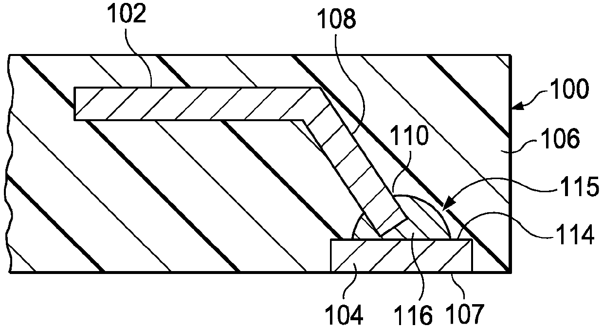
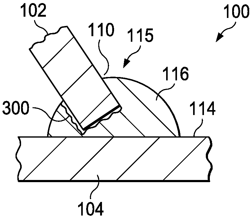
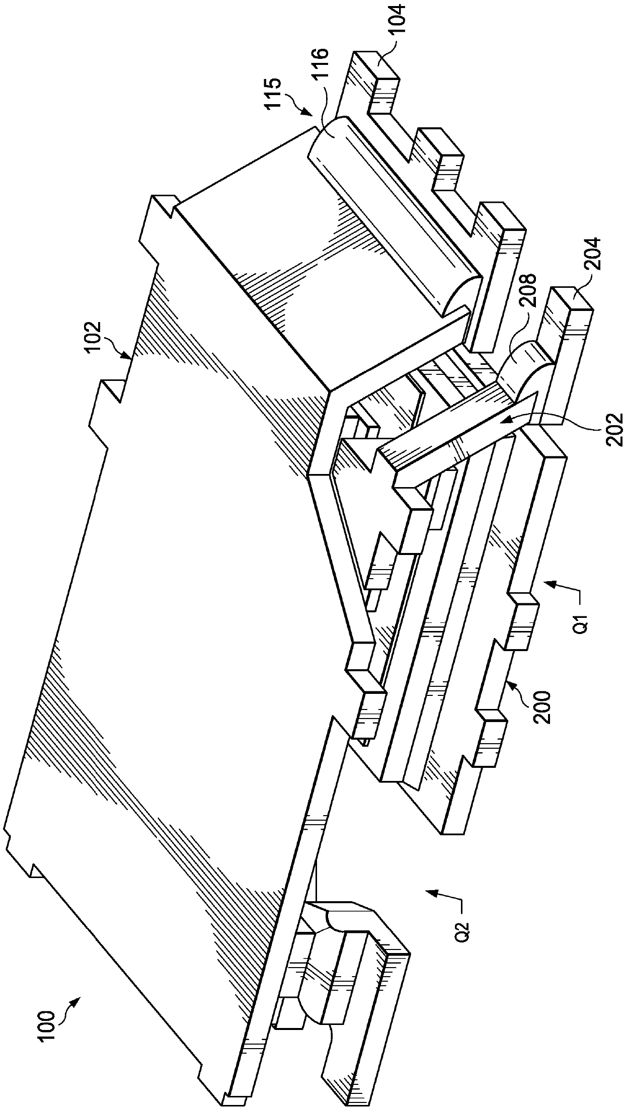
[0014] figure 1 is a side cross-sectional view of a portion of electronic device 100 showing the bond between clip 102 and lead 104 . Examples of device 100 include integrated circuits in quad flat no-lead (QFN) packages or dual flat no-lead (DFN) packages. Clip 102 is a conductive material such as copper that is coupled to at least one electronic component ( figure 1 not shown). In some embodiments, clip 102 is electrically coupled to the source or drain of at least one field effect transistor (FET). Leads 104 are also conductive material and serve as leads of device 100 to couple device 100 to other electronic devices. For example, leads 104 may electrically and mechanically couple device 100 to conductors on a printed circuit board.
[0015] The device 100 is embedded in a mold 106 applied by conventional molding techniques. Leads 104 have surfaces 107 not surrounded by mold 106 and serve as conductive pads for device 100 . During assembly of device 100 to a printed c...
PUM
 Abstract
Description
Claims
Application Information
 - R&D
- Intellectual Property
- Life Sciences
- Materials
- Tech Scout
- Unparalleled Data Quality
- Higher Quality Content
- 60% Fewer Hallucinations
Browse by: Latest US Patents, China's latest patents, Technical Efficacy Thesaurus, Application Domain, Technology Topic, Popular Technical Reports.
© 2025 PatSnap. All rights reserved.Legal|Privacy policy|Modern Slavery Act Transparency Statement|Sitemap|About US| Contact US: help@patsnap.com