Supercharge Your Innovation With Domain-Expert AI Agents!

a display device

A display device and display area technology, applied in the direction of instruments, nonlinear optics, optics, etc., can solve the problems of reduced production capacity, increased cost, and inability to detect in time to confirm the yield status, etc.

Active Publication Date: 2020-12-18
AU OPTRONICS KUNSHAN CO LTD
View PDF13 Cites 0 Cited by
  • Summary
  • Abstract
  • Description
  • Claims
  • Application Information

AI Technical Summary

Problems solved by technology

[0005] 1. Every time a product with a different resolution is changed, it takes 1 to 2 hours to replace and confirm the fixture, resulting in a decrease in production capacity;
[0006] 2. For each product with different resolutions, 4 to 8 fixtures need to be prepared, and the number of fixtures will be large, resulting in an increase in cost;
[0007] 3. It takes 1 to 2 months to make a fixture suitable for one resolution, and the new product stage may not be able to detect in time to confirm the yield status

Method used


Image

  • a display device
  • a display device
  • a display device

Examples


Embodiment Construction

[0051] In order to make the above objects, features and advantages of the present invention more comprehensible, specific implementations of the present invention will be described in detail below in conjunction with the accompanying drawings. In the following description, numerous specific details are set forth in order to provide a thorough understanding of the present invention. However, the present invention can be implemented in many other ways different from those described here, and those skilled in the art can make similar improvements without departing from the connotation of the present invention, so the present invention is not limited by the specific embodiments disclosed below.

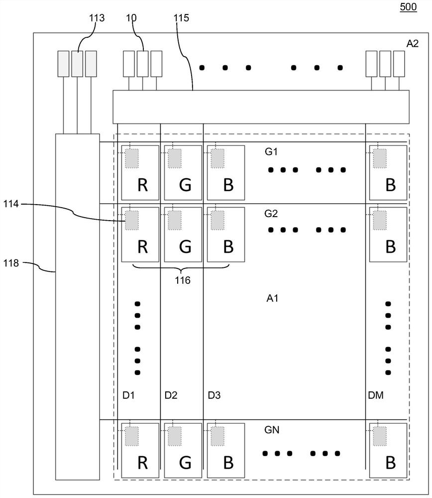
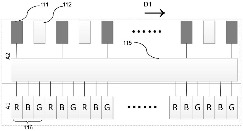
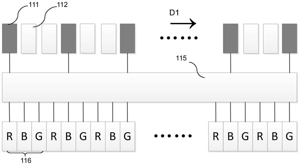
[0052] figure 1 It is a schematic top view of a display device in the prior art. Such as figure 1 As shown, a display device 100 mainly includes a first substrate (such as a TFT substrate), a second substrate (such as a CF substrate), and a display molecular layer (such as liquid crysta...


PUM


Abstract

A display device includes: a first substrate, a second substrate and a display molecule layer disposed between said first substrate and said second substrate; a plurality of thin film transistors disposed on the display area of said first substrate; a plurality of gate lines respectively electrically connected to the control terminal of said thin film transistor; a plurality of data terminals located on the peripheral area and respectively electrically connected to the first terminal of said thin film transistor; and a plurality of virtual terminals located in the peripheral area and respectively electrically insulated from each of said thin film transistors; wherein said data terminals and said virtual terminals are staggered along a first direction.

Description

technical field [0001] The invention relates to the field of display design, in particular to the design of a test pad (Array Test Pad) in the display and a display device using the test pad. Background technique [0002] Thin Film Transistor Liquid Crystal Display (TFT-LCD, Thin Film Transistor Liquid Crystal Display) is a common display, TFT-LCD is an active matrix liquid crystal display, and the liquid crystal pixels on the TFT-LCD are driven by thin film transistors, that is, through Active switches are used to achieve independent and precise control of each pixel, so that high-speed, high-brightness, high-contrast display screen information can be achieved to achieve fine display effects. [0003] The structure of TFT-LCD mainly includes CF substrate, TFT substrate and liquid crystal material. In the production process of the TFT-LCD panel, it is an important step to check the electrical characteristics of the TFT substrate. In the prior art, an Array Tester (Array Te...

Claims


Application Information

Patent Timeline
Patent Type & Authority Patents(China)
IPC IPC(8): G02F1/1345G02F1/13
CPCG02F1/1309G02F1/1345
Inventor 何孟修曾弘岳赖骏凱
Owner AU OPTRONICS KUNSHAN CO LTD
Features
  • R&D
  • Intellectual Property
  • Life Sciences
  • Materials
  • Tech Scout
  • Unparalleled Data Quality
  • Higher Quality Content
  • 60% Fewer Hallucinations
Learn More