Display panel, manufacturing method thereof and display device

A display panel and substrate technology, applied in the direction of instruments, nonlinear optics, optics, etc., can solve problems such as difficult to achieve frameless design, achieve the effect of frameless design and reduce the degree of reflection

Active Publication Date: 2018-06-12
HUIZHOU CHINA STAR OPTOELECTRONICS TECHNOLOGY CO LTD
View PDF7 Cites 21 Cited by
  • Summary
  • Abstract
  • Description
  • Claims
  • Application Information

AI Technical Summary

Problems solved by technology

[0004] The LCD panel is placed on the back panel. Due to the presence of the Bonding area of ​​the array substrate, the size of the array substrate of the LCD panel will be larger than the size of the color filter substrate. The Bonding area of ​​the array substrate protrudes toward the side, and the frame needs to be designed to Therefore, the traditional LCD panel needs to use complex optical components to cover the border of the non-display area, and it is difficult to achieve a true borderless design.

Method used


Image

  • Display panel, manufacturing method thereof and display device
  • Display panel, manufacturing method thereof and display device
  • Display panel, manufacturing method thereof and display device

Examples


Embodiment Construction

[0027] In order to make the objectives, technical solutions and advantages of the present invention clearer, the following further describes the present invention in detail with reference to the accompanying drawings and embodiments. It should be understood that the specific embodiments described here are only used to explain the present invention, but not to limit the present invention.

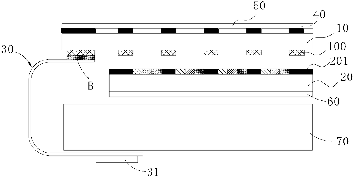
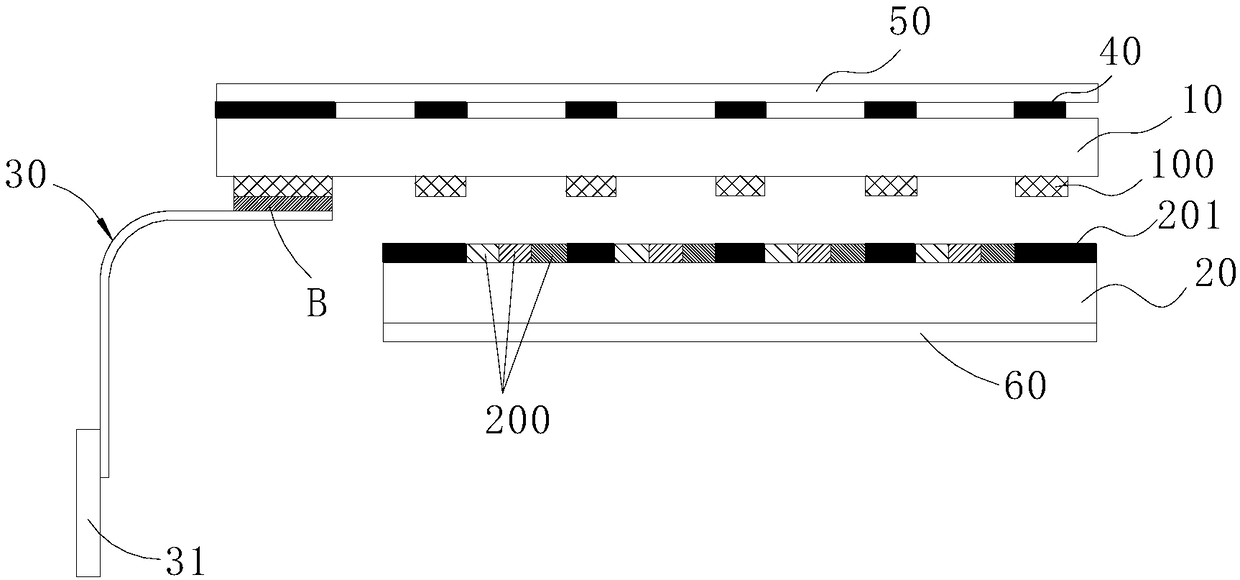
[0028] See figure 1 with figure 2 The display device of the embodiment of the present invention includes a backlight module 70 and a display panel disposed above the backlight module 70. The display panel includes a first substrate 10, a second substrate 20, a flip chip film 30, and a light-shielding array layer 40. The substrate 10 is opposed to the second substrate 20 and is arranged at intervals, and one end of the first substrate 10 extends beyond the second substrate 20 to form a binding end. The flip chip film 30 is bound on the surface of the binding end facing the second substrate 20 an...


PUM


Abstract

The invention discloses a display panel, a manufacturing method thereof and a display device. The display panel comprises a first substrate, a second substrate, a chip-on-film and a light shading array layer, wherein one end of the first substrate exceeds the second substrate to form a binding end; the chip-on-film is bound on the inner side of the binding end; a metal signal wire which is positioned in a non-pixel region is arranged on the inner surface of the first substrate; and the light shading array layer is positioned in the non-pixel region and completely shades the metal signal wire.Because the first substrate faces a looker and the chip-on-film is bound on the inner side of the binding end of the first substrate, frameless design is realized; the patterning light shading array layer is arranged on the outer surface of the first substrate, a pattern which corresponds to the metal signal wire on the inner surface of the first substrate is formed by the light shading array layer to cover the metal signal wire, when entering the display panel, external environment light can be weakened or obstructed in the light shading array layer, the light intensity which can reach the metal signal wire is greatly weakened, and therefore, the reflection degree of the metal signal wire is reduced.

Description

Technical field [0001] The present invention relates to the field of liquid crystal display technology, in particular to a display panel, a manufacturing method thereof, and a display device. Background technique [0002] With the rapid development of LCD (Liquid Crystal Display) panels, LCD displays have gradually become the mainstream of display technology due to their ultra-thin, light weight, non-radiation, and stable performance. [0003] Borderless displays are not necessarily frameless. The liquid crystal panel of the display usually includes a color film (CF) substrate and an array (TFT Array, or thin film transistor array) substrate. Liquid crystal is filled between the two. In the traditional In the overall design of the borderless display, the color filter substrate side faces outward and the array substrate side faces the backlight source, that is, the color filter substrate of the liquid crystal panel is seen by the naked eye when the final user looks at it. [0004] Th...

Claims


Application Information

Patent Timeline
Patent Type & Authority Applications(China)
IPC IPC(8): G02F1/1345G02F1/1335G02F1/1362G02F1/1333
CPCG02F1/1333G02F1/133512G02F1/13452G02F1/136209G02F1/136286G02F1/133514G02F1/133528
Inventor 阙成文樊勇
Owner HUIZHOU CHINA STAR OPTOELECTRONICS TECHNOLOGY CO LTD
Why Eureka
Try Eureka