
superconducting wire

A technology of superconducting wires and superconducting materials, which is applied in the field of superconducting wires and can solve the problems that the ceramic layer cannot generate stress, etc.

Active Publication Date: 2020-01-21
SUMITOMO ELECTRIC IND LTD
View PDF6 Cites 0 Cited by
  • Summary
  • Abstract
  • Description
  • Claims
  • Application Information

AI Technical Summary

Problems solved by technology

However, the ceramic layer cannot generate stress

Method used


Image

  • superconducting wire
  • superconducting wire
  • superconducting wire

Examples


specific Embodiment approach

[0049] Embodiments of the present invention will be described below based on the drawings. In the following drawings, the same or corresponding parts are denoted by the same reference numerals, and description thereof will not be repeated.

no. 1 example

[0051] Construction of Superconducting Wires

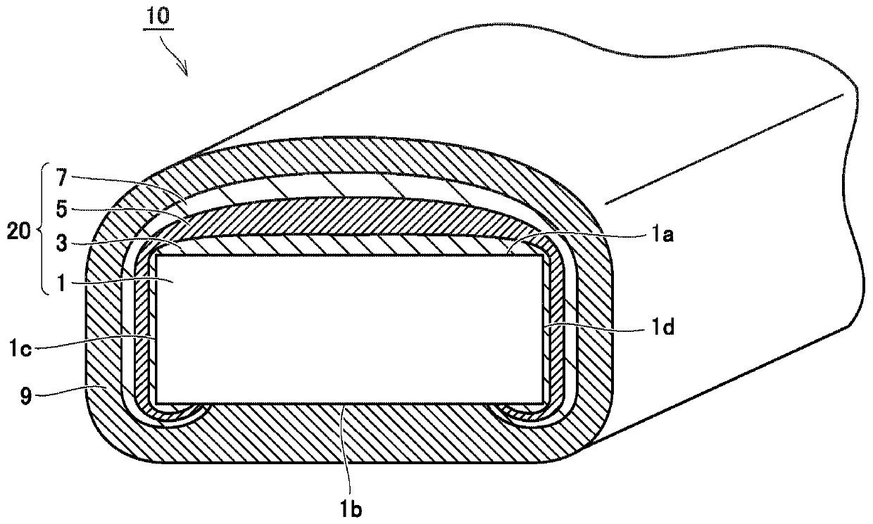
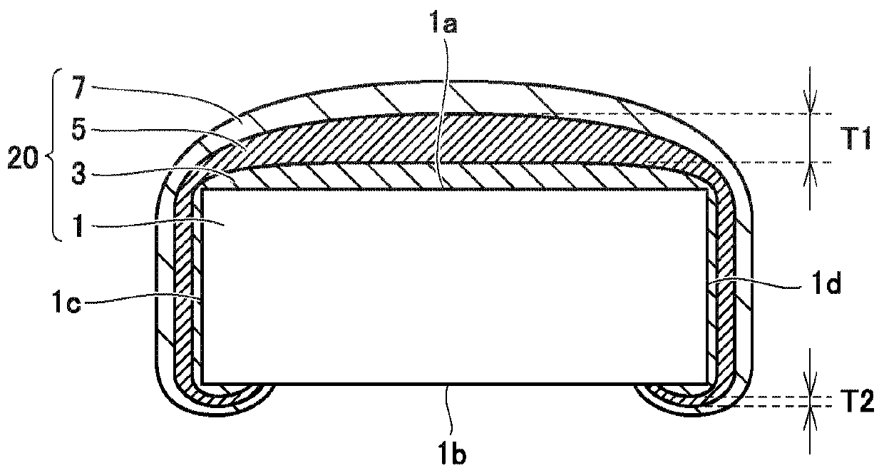
[0052] figure 1 is a schematic cross-sectional view showing the configuration of the superconducting wire in the first embodiment. figure 1 A section in a direction transverse to the direction in which superconducting wire 10 extends in the first embodiment is shown. Therefore, the direction transverse to the plane of the drawing is the longitudinal direction of the superconducting wire, and the superconducting current in the layer 5 of superconducting material flows in the direction transverse to the plane of the drawing. In addition, in figure 1 And in the schematic cross-sectional views in subsequent figures, in order to facilitate easy recognition of the drawings, the distance between the dimension in the vertical direction (hereinafter also referred to as "thickness direction") and the dimension in the left-right direction (hereinafter also referred to as "width direction") is shown. The difference is small. However, in r...

no. 2 example

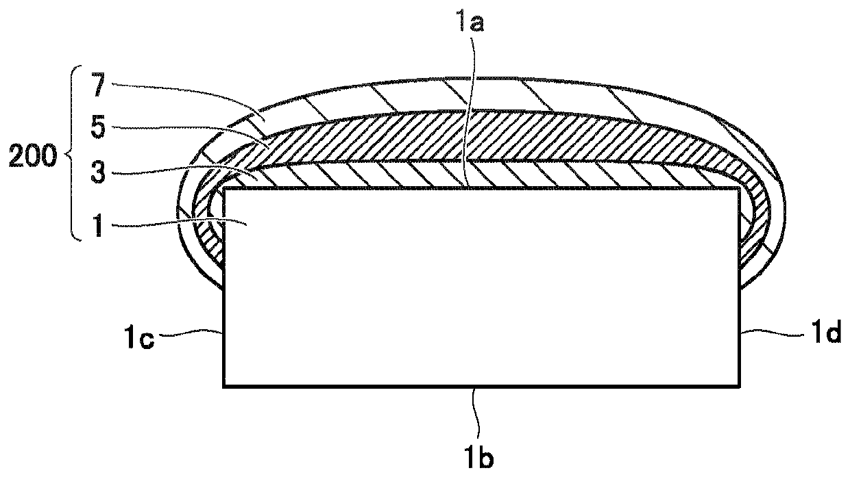
[0109] Figure 11 is a schematic cross-sectional view showing the configuration of a superconducting wire 10C in the second embodiment. Figure 11 A cross section in a direction transverse to the direction in which superconducting wire 10C extends is shown.

[0110] refer to Figure 11 , except that the structure of the multilayer stack 20 differs from figure 2 In addition to the structure of the multilayer stack 20 shown, basically the superconducting wire 10C in the second embodiment has the same figure 1 The superconducting wire 10 shown has a similar structure.

[0111] In the superconducting wire 10C, the intermediate layer 3, the superconducting material layer 5, and the protective layer 7 on the first main surface 1a protrude at opposite ends in the width direction, respectively, and thus have a central portion retracted in the width direction thereof. section. In other words, the upper surface of each of intermediate layer 3 , superconducting material layer 5 and...


PUM

PropertyMeasurementUnit
sizeaaaaaaaaaa
thicknessaaaaaaaaaa
thicknessaaaaaaaaaa

Abstract

A superconducting wire (10) comprises a substrate (1) and a superconducting material layer (5). The substrate (1) comprises a first main surface (1a) and a second main surface (1b) opposite the first main surface (1a). The layer (5) of superconducting material is arranged on the first main surface (1a). Along at least a part of the superconducting wire (10) in the direction in which the superconducting wire (10) extends, the superconducting material layer (5) is arranged to cover the substrate (1) along the width direction The side surface of the substrate (1) and covers at least a part of the second main surface (1b). The thickness of the superconducting material layer (5) on the first main surface (1a) varies along the width direction. The maximum thickness of the superconducting material layer (5) on the second main surface (1b) is smaller than the maximum thickness of the superconducting material layer (5) on the first main surface (1a).

Description

technical field [0001] The present invention relates to a superconducting wire, and more particularly to a superconducting wire in which a superconducting material layer is formed on a substrate. Background technique [0002] In recent years, superconducting wires in which a superconducting material layer is formed on a metal substrate are being developed. In particular, oxide superconducting wires have attracted attention. The oxide superconducting wire includes a layer of a superconducting material made of an oxide superconductor, which is a high-temperature superconductor having a transition temperature equal to or higher than the temperature of liquid nitrogen. [0003] Such an oxide superconducting wire is generally manufactured by forming an intermediate layer on an orientation-aligned metal substrate, forming an oxide superconducting material layer on the intermediate layer, and further forming a stabilizing layer of silver (Ag) or copper (Cu) (See, for example, Jap...

Claims


Application Information

Patent Timeline
Patent Type & Authority Patents(China)
IPC IPC(8): H01B12/06H10N60/85H10N60/01
CPCH01B12/06Y02E40/60H10N60/857H10N60/0576H10N60/0801
Inventor 山口高史永石龙起小西昌也山名健司本井见二
Owner SUMITOMO ELECTRIC IND LTD
Learn More