Electronic packaging structure

A technology of electronic packaging and electronic components, applied in the field of electronic packaging structures that can improve reliability, can solve problems such as uneven pressure, incomplete sintering, hollowing out, etc., and achieve the effect of preventing cracking and improving the effect

Inactive Publication Date: 2018-08-21
IND TECH RES INST
View PDF6 Cites 0 Cited by
  • Summary
  • Abstract
  • Description
  • Claims
  • Application Information

AI Technical Summary

Problems solved by technology

[0007] However, the large-sized semiconductor chip 14 is sintered and bonded using the silver bonding layer 11. The periphery of the bonding layer 11 is often caused by incomplete sintering due to uneven pressure and many pores are formed, and the manufacturing process is often limited by the printing and coating method. influence, the peripheral bottom of the bonding layer 11 will be partially hollowed out, so the above-mentioned

Method used


Image

  • Electronic packaging structure
  • Electronic packaging structure
  • Electronic packaging structure

Examples


Embodiment Construction

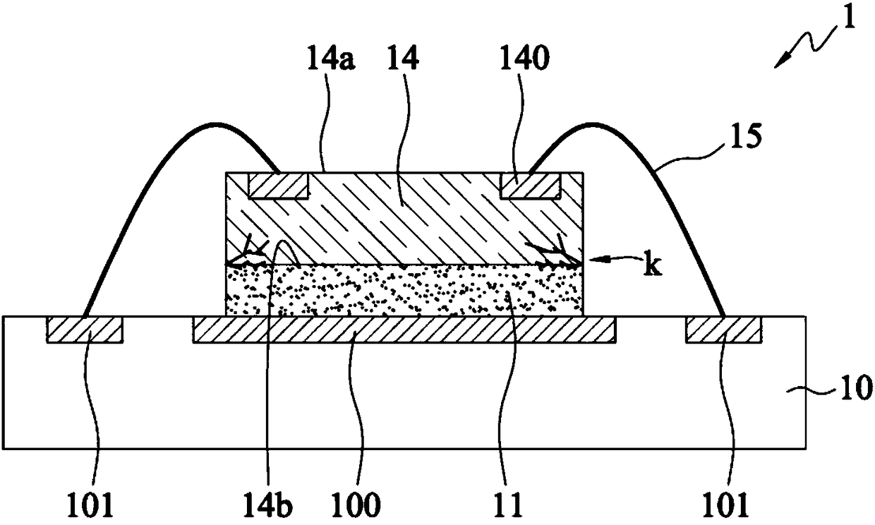
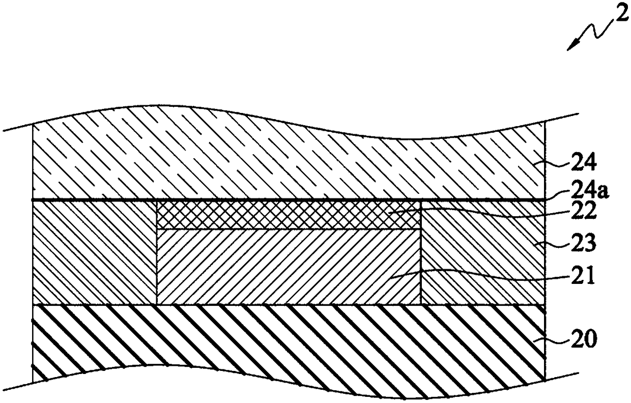
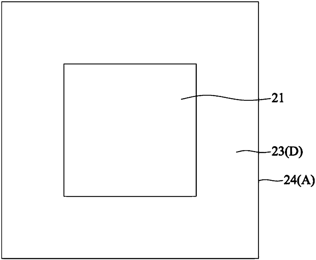
[0040] The following specific examples illustrate the implementation of the present invention. Those familiar with this technology can easily understand other advantages and effects of the present invention from the content disclosed in this specification.

[0041] It should be noted that the structure, ratio, size, etc. shown in the drawings attached to this specification are only used to match the content disclosed in the specification for the understanding and reading of those familiar with this technology, and are not intended to limit the scope of the present invention. The limited conditions of implementation do not have technically substantial significance. Any structural modification, proportional relationship change, or size adjustment should still fall within the scope of the present invention without affecting the effects and objectives that can be achieved. The technical content disclosed in the present invention can be covered within a range. At the same time, terms ...


PUM


Abstract

An electronic package structure is provided. The electronic packaging structure binds a chip on a metal boss of a bearer and stress buffering material surrounds the metal boss to serve as a stress buffering portion, so as to enhance the effect of stress buffering, thereby preventing a wafer from cracking due to stress.

Description

Technical field [0001] The invention relates to an electronic packaging structure, in particular to an electronic packaging structure capable of improving reliability. Background technique [0002] With the vigorous development of the electronics industry, electronic products are gradually moving towards the trend of multi-function and high performance. Technologies currently applied in the field of chip packaging, such as Chip Scale Package (CSP), Direct Chip Attached (DCA) or Multi-Chip Module (MCM) Such as flip-chip packaging modules, or three-dimensional stacking and integration of chips into three-dimensional integrated circuit (3D IC) chip stacking technology. [0003] In the existing semiconductor packaging technology, for example, figure 1 As shown in the wire-bonding packaging technology, the semiconductor packaging structure 1 is bonded to a semiconductor chip 14 (the main material is silicon, for example, by bonding layer 11 (for example, glue) on the die pad 100 of a p...

Claims


Application Information

Patent Timeline
IPC IPC(8): H01L23/00H01L23/488
CPCH01L23/488H01L23/562H01L2224/29012H01L24/83H01L2224/29013H01L2224/29076H01L2224/291H01L2224/32245H01L2224/83192H01L2224/83204H01L2224/83439H01L2224/83444H01L2224/83447H01L2224/83455H01L2224/8381H01L24/05H01L24/29H01L24/32H01L2224/29139H01L2224/29147H01L2224/29155H01L2224/32503H01L2924/3512H01L2924/014H01L2924/00014H01L2924/00012
Inventor 张景尧张道智吕芳俊韩伟国高国书
Owner IND TECH RES INST
Why Eureka
Try Eureka