
Array substrate, display panel and display device

An array substrate, display scanning technology, applied to static indicators, instruments, computing, etc., can solve the problems of increasing the frame width of the display device, the influence of the distribution of the gate drive circuit, and affecting the display effect of the display device. Affect, display high effect

Active Publication Date: 2020-10-02
XIAMEN TIANMA MICRO ELECTRONICS
View PDF5 Cites 0 Cited by
  • Summary
  • Abstract
  • Description
  • Claims
  • Application Information

AI Technical Summary

Problems solved by technology

However, the frame area of ​​the display device is also provided with a gate drive circuit for driving the display, and the way of disposing the fingerprint drive circuit in the frame area of ​​the display device will not only increase the width of the frame of the display device, but also does not conform to the narrow frame. At the same time, it also affects the distribution of the gate drive circuit, which may affect the display effect of the display device

Method used


Image

  • Array substrate, display panel and display device
  • Array substrate, display panel and display device
  • Array substrate, display panel and display device

Examples


Embodiment Construction

[0028] The following will clearly and completely describe the technical solutions in the embodiments of the present invention with reference to the accompanying drawings in the embodiments of the present invention. Obviously, the described embodiments are only some, not all, embodiments of the present invention. Based on the embodiments of the present invention, all other embodiments obtained by persons of ordinary skill in the art without making creative efforts belong to the protection scope of the present invention.

[0029] As mentioned in the background art, fingerprint recognition needs to add a fingerprint driving circuit corresponding to the fingerprint sensing electrode. In the prior art, the fingerprint driving circuit is all arranged in the frame area of ​​the display device. However, the frame area of ​​the display device is also provided with a gate drive circuit for driving the display, and the way of disposing the fingerprint drive circuit in the frame area of ​​...


PUM


Abstract

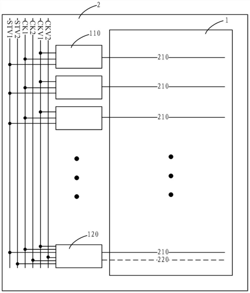
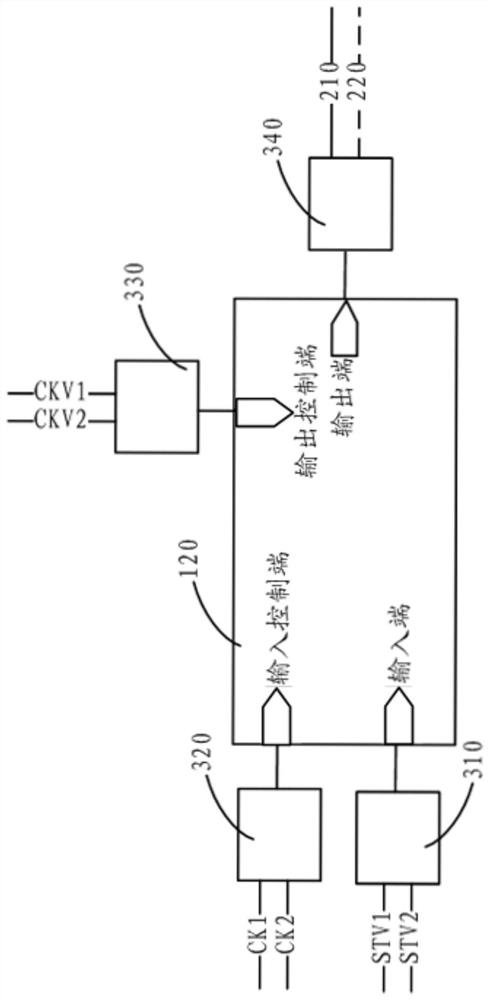
The invention discloses an array substrate, a display panel and a display device. By multiplexing part of the display shift registers of the display gate drive circuit into a multiplexed shift register, the display can be started according to the display sequence signal included in the display scanning stage. Under the control of the start signal, the display start clock signal and the display output clock signal, the display shift register outputs the display scan signal, and in the fingerprint scanning stage, according to the fingerprint start signal, the fingerprint start clock signal and the fingerprint output clock signal included in the fingerprint timing signal Under the control of the multiplexing shift register, the fingerprint scanning signal is output, so that the display device can complete the functions of display and fingerprint identification, avoiding the problem of increasing the frame width of the display device by adding too many fingerprint drive circuits in the frame area of ​​the display device The problem is in line with the development trend of narrow borders; at the same time, the impact on the distribution of the display gate drive circuit is reduced, the impact on the display effect of the display device is reduced, and a high display effect is ensured.

Description

technical field [0001] The present invention relates to the field of display technology, and more specifically, to an array substrate, a display panel and a display device. Background technique [0002] The fingerprint of the human body has uniqueness and invariance, which makes the security performance of fingerprint identification stronger. At the same time, because of its simple operation, it is widely used in various fields, for example, the field of display technology. In the field of display technology, taking a mobile phone as an example, operations such as unlocking the mobile phone or opening a specific application program of the mobile phone can be completed through fingerprint recognition. However, fingerprint recognition needs to add a fingerprint driving circuit corresponding to the fingerprint sensing electrode, and in the prior art, the fingerprint driving circuit is arranged in the frame area of ​​the display device. However, the frame area of ​​the display ...

Claims


Application Information

Patent Timeline
Patent Type & Authority Patents(China)
IPC IPC(8): G09G3/36G06K9/00
CPCG09G3/3674G06V40/12
Inventor 蔡寿金朱绎桦陈国照
Owner XIAMEN TIANMA MICRO ELECTRONICS
Learn More